 land-boards.com
Grant Searle has a third software build that might prove handy towards having external flash card storage. This is the software that he uses with his Z80 on an inexpensive FPGA project. This is named the Multicomp project.
I got this third build working in minutes.
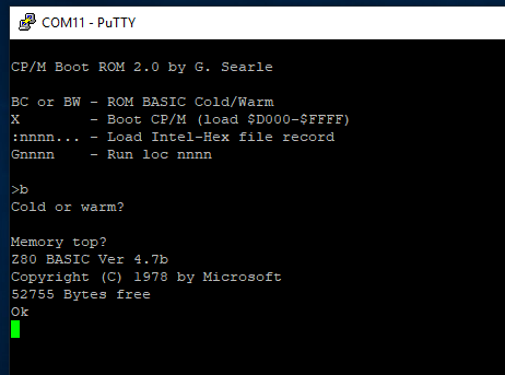
It only took a bit of messing around since Grant's stock software assumes two ACIA (M6850 parts). I copied the M6580 code that I made for the previous logs and deleted most of the guts of the lower level routines. The read status routine returns saying that there are no characters in the second ACIA. That is how Grant chooses between the two serial ports - whichever port returns the space is selected as the code default - handy solution to the problem. Without this added code Grant's software hangs on the access to the missing 2nd ACIA.
Why Yet Another Build of Grant's software?
This is another 56KB SRAM (in BASIC) build but with critical differences. Grant's 48K build supports an assembly language monitor and CP/M. Grant's other 56K build only supports NASCOM BASIC (no CP/M). This build supports both NASCOM BASIC and CP/M support all packed into an 8K PROM space. That's cool because it's getting 8KB more of program space for BASIC with the cost of losing the machine code monitor. Not a real big cost but I could always load the old build if I wanted to mess around with the monitor.
What I really wanted from this build is Grant's hardware/software support for CP/M that he has in the FPGA. In Grant's discrete (non-FPGA designs) he uses an external Compact Flash (CF) card which requires a bunch of connections from the CPU bus and these are expensive I/O on an FPGA. For the FPGA version, Grant uses an SD card which only needs a 4-pin SPI bus to control it. And the PSoC also has an SPI bus and 4 spare connectorized pins so it should be possible to get an SD card working with this software build. I say possible since it's yet to be done but this is where we are headed next.
Grant's Documentation for the SD Card Interface
Grant has some instructions on his page about the SD card on this page and the other support that is needed to do this (at least how he did it with his FPGA solution).
Trading Spaces
The first thing is that the memory mapper needs to swap out the EPROM for SRAM when the program writes to a particular memory location.
When CP/M starts, the ROM is to be disabled.
The CP/M images are set up so that a write to $38 will
turn off the ROM, resulting in ALL of the 64K address space
being the SRAM instead.
This is almost unneeded with this board design. The reason is there's no actual EPROM on the card - all memory is already SRAM. And CP/M uses SRAM. I say almost because Warm Boot complicates that. If CP/M overwrote the data in the first 8K then the board can't boot back into the initial prompt and run BASIC without reloading the code. That really would be no big deal but supporting page swapping shouldn't be difficult since the hardware is present already to do the swap.
Although there is hardware support in the PSoC for page mapping and swapping but it hasn't been used yet. The PSoC code does test all 512KB of SRAM when it powers up so we know the SRAM is working. What is missing is the I/O routine to deal with the swapping.
Adding the I/O handler for the swap write should be similar to the other handlers. To start with a #define for this memory mapper would look like in Hardware_Config.h:
#ifdef GRANT_FPGA_CPM // Swap out first 8KB
I named it _1 since there will likely be any number of memory mapping schemes employed with this hardware.
It is set to undefined at the top of the file and then defined within the particular build section of the file that corresponds to this build - noted by:
#ifdef GRANT_FPGA_CPM
This then gets added to this section as:
    #define USING_MEM_MAP_1
    #ifdef USING_MEM_MAP_1
        #define MEM_MAP_SWAP        0x38
    #endif
The code to deal with this gets added to Z80_IO_Handle.c as a new switch case statements. The code to perform the I/O handler needs to be written, let's put in a stub for now called write_mem_map_1.
#ifdef USING_MEM_MAP_1
        case MEM_MAP_SWAP:
            if (ioCrtlRegVal == REGULAR_WRITE_CYCLE)      // regular write cycle
            {
                write_mem_map_1();
                return;
            }
#endif
Now that we have a need for a routine it is a good time to create a .c and .h file for memory mapper routines. Let's call these Z80_Mem_Mappers.c and .h. In addition to this function, they will contain any memory mappers we might need in the future. Remember we have 512KB of SRAM and this only uses one additional page.
There are a couple of registers in the PSoC that need to be dealt with to swap pages. An earlier log entry (Z80 Memory Mapping/Bank Switching) described the design intent earlier for this project. There are some registers that need to be initially set (are possibly already set) so an initialization function would be smart to create at this point. That way we know where we are starting from.
The BankBaseAdr register sets the base address of the comparison. For this built it needs to be set to 0x00 initially and it will never change.
The BankMask register is set for the bank size per the table on the schematic:
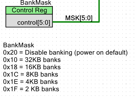
We want an 8K bank so we need to set the BankMask to 0x1C. This also should not change after it is initialized.
At the end of the logic on that page this means that any access to the first 8KB of addresses will result in the BANKED signal being asserted. When BANKED is asserted it causes the upper SRAM addresses to come from the AdrHighOut register. This implies that AdrHighOut should have contents of 0x00 until the swap control word is written. So, this means that the initialization values of the registers are:
- BankBase 0x00
- BankMask 0x1C
- AdrHighOut 0x00
It almost doesn't matter what value is given for the upper address lines when BANKED is selected. To swap to another page we just need to set one of the higher bits A[18..15] to 1. For this build let's just load the AdrHighOut with 0x20 when the bank selection address is written from the Z80. The intialization code looks like:
void init_mem_map_1(void)
{
    BankBaseAdr_Write(0x00);
    BankMask_Write(0x1c);
    AdrHighOut_Write(0x00);
}
The function to perform the memory map swap looks like
void write_mem_map_1(void)
{
    AdrHighOut_Write(0x20);     // Set A18..A16 to 0x1
    ackIO();
}
This code compiles without error.
Testing the Bank Swapping
When Grant's code loads CP/M it does fetches from the SD card and loads the code into the CP/M address space at 0xD000. He describes this in the address map as:
Once CP/M is loaded

0000-FFFF RAM

0100 Transient program area (applications)
D000 CP/M System
E600 BIOS
This will be challenging to test since it will require the SD card code to work in order to verify it works. Grant includes some source code but is lacking the critical code for this function.
There's little visibility into the mapper from the PSoC code. Remapping the LED out of the control register it is contained in and onto the BANKED line might be one way of having a visual indication that the bank memory is being accessed.
Another way to test this might be to write a piece of code to see if it works. The test code would need to run in higher memory and do read/writes of the lower memory. That's possible but sounds like more work than I want.
In the next log we'll take a look at Grant's code for loading CP/M and see how it work with the SD card.
Discussions
Become a Hackaday.io Member
Create an account to leave a comment. Already have an account? Log In.