 sjm4306
To start off, thanks to JLCPCB for sponsoring this project as well as providing pcbs to get the ball rolling. JLCPCB Prototype for $2 (Any Color): https://jlcpcb.com
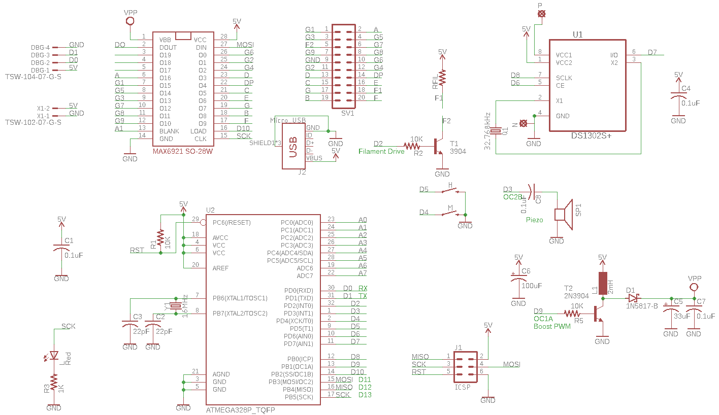
The hardware requirements of this project are fairly simple: two buttons for setting time, a small speaker for delightful beeps and possibly to add alarm functionality in the future, onboard software controllable "high voltage" boost converter to generate ~30-70V from 5V, USB micro power input, battery backed real time clock, and software controllable dc filament drive/driver blanking. I've pretty much done an identical clock in the past using a larger IV-18 tube with the pcb done on protoboard using hand wiring but this time I wanted something that would look more professional.
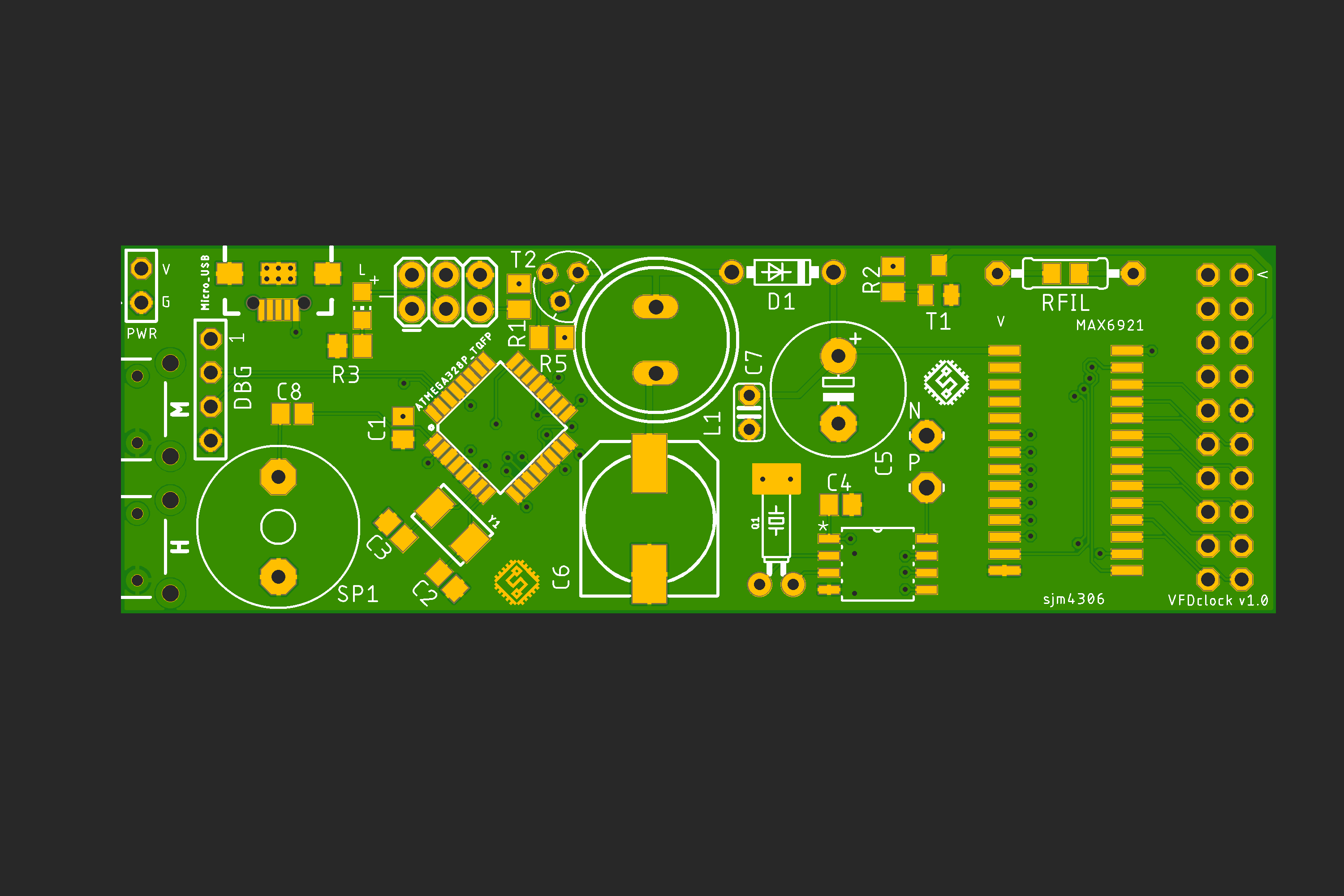
The design consists of two boards. The first is the main board that contains all the electronics to keep time, generate the necessary tube drive voltage, and control all the multiplexed segments for the display. I wanted to keep the board small, single sided for easy assembly, and yet not go crazy with microscopic surface mount components. The digital parts are for the most part surface mount, but the boost converter components are through hole and suitably spaced for ease of replacement or sourcing suitable alternatives. All the low voltage stuff is condensed to the left hand side, while the higher voltage goodies lie on the right side with the tube header on the very end. I opted to just do dc filament drive as my past experience with the brightness gradient due to dc wasn't bad (especially for small tubes like these) compared to the complication that moving to ac drive would add. Here's the circuit and layout I settled on:
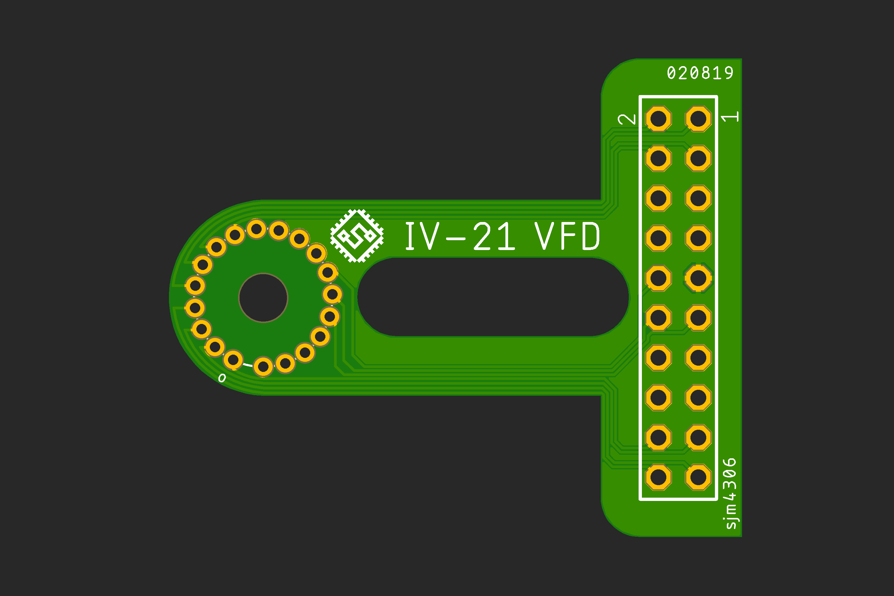
The second board is just a wiring pass through to allow the vfd to be mounted above the main board, and connects via a standard 0.1" pin header and female socket for ease of replacement (just in case the tube burns out or meets an unfortunate end after a rough bump or drop). Here's what it looks like:
I actually had an interesting time figuring out an easy way to calculate the positions of the radial pads. Since eagle does everything in cartesian coordinates making a nice evenly spaced circular arrangement of pads is easier said than done. I'm not familiar with eagle's scripting language yet, so I ended up manually setting the coordinates of each pad, but to make my life easier I wrote up a quick excel spreadsheet to calculate the x and y values for you if you plug in the desired number of pins, radius and angular separation. Hah, and I often hear people say they never use trig after high school, but those equations came in handy for me now! Then all you need to do is plug in the output x and y coordinates into the pad position settings in eagle and they are perfectly aligned! (Caveat: the calculations sometime spit out negative angles and positions in the wrong quadrant, but some common sense of signs when transferring the coordinates will fix those issues quick enough)
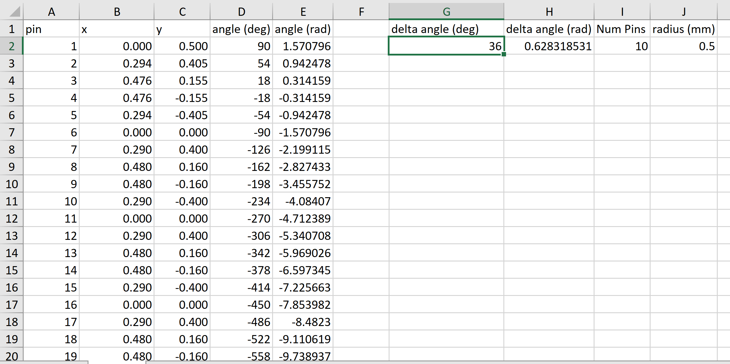
This "calculator" ended up being super useful and I will definitely end up using it in future projects with various tubes I intend to use.
After receiving the boards from JLCPCB I quickly assembled them.
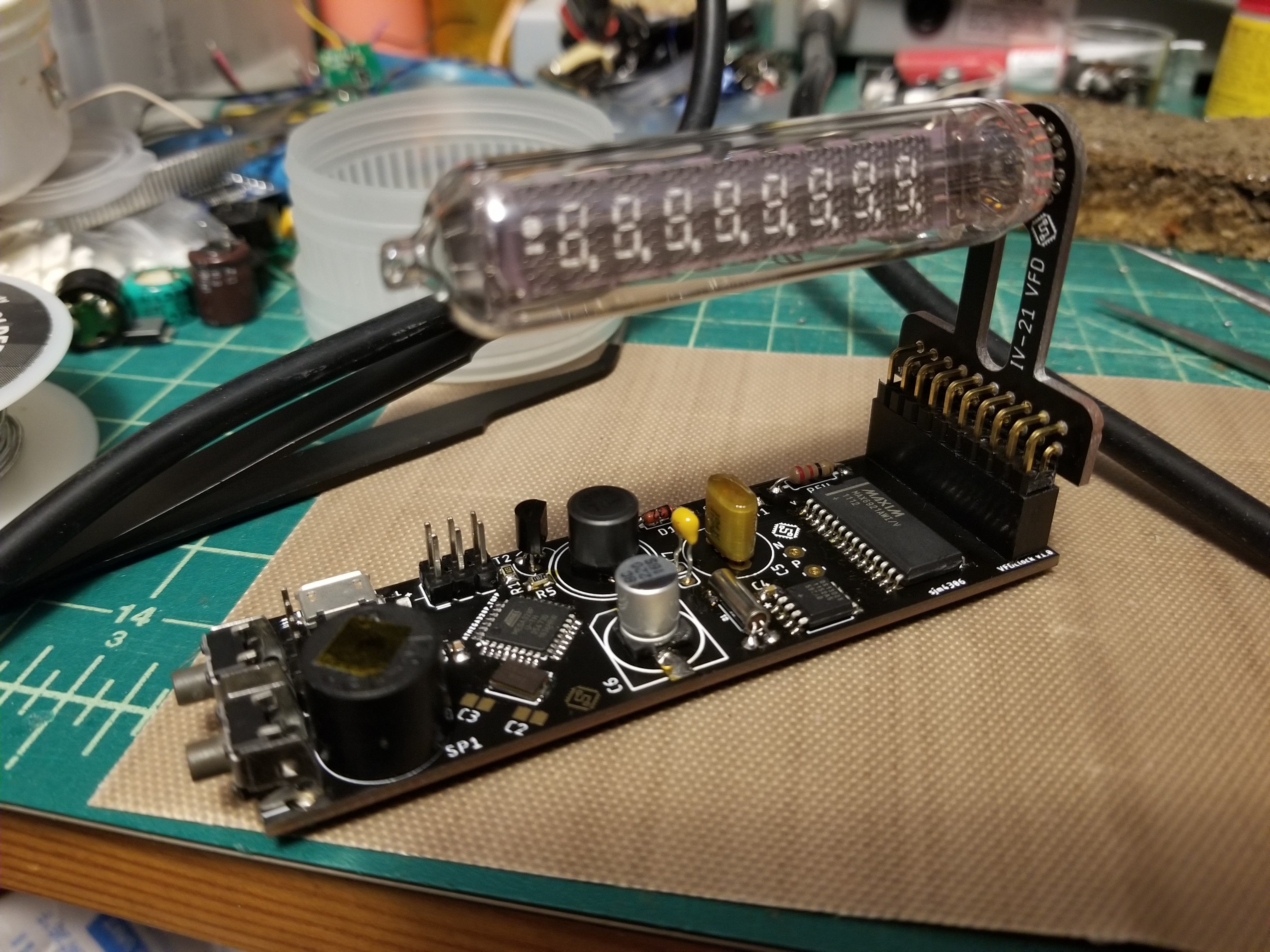
It certainly looks the part! There were a few small problems with the circuit though. I accidentally miswired c6 (the large electrolytic cap) to the wrong point (just after the switching transistor instead of the 5V input DOH!) so the boost converter wasn't able to ... erm boost. I cut the trace and off she went, easily generating over 100V off the 5V input. The second issue I ran across is that I wired the blanking input of the max6921 hv driver chip to the atmega's miso pin. This didn't seem like it'd be an issue, but apparently when the atmega is configured as a master SPI device the mico pin is hardwired to be an input and cannot be reconfigured to use as an output. Bummer, but I lifted the max6921 pin and ran a bodge wire the the open A1 output pin of the atmega and all was well. I've already fixed the pcb files for these two errors so don't worry.
Finally with all the hardware properly assembled I could start writing the firmware. In the next log I'll talk a bit about the software and post the assembly/demo video.
Discussions
Become a Hackaday.io Member
Create an account to leave a comment. Already have an account? Log In.