 Chris Chung
Calculator Functions and Features
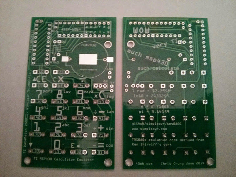
As this project emulates the original TI DataMath and Sinclair Scientific calculators, it operates exactly the same as the original ones. The keyboard layouts are similar in both calculators. On the PCB, the dominant key legends (on top of each key) are for TI DataMath, while the smaller legends (top and slightly left of each key) are for Sinclair Scientific emulating.
I had select the MCU clock speed to be 8 Mhz, which appears to more or less matches the speed of the original calculators. I only observe the speed of the original calculators on youtube videos.
DataMath instructions
Latest firmware now does LPM4 auto-off, can eliminate SPDT slide switch on pcbAuto-off time is 60 seconds of inactivity. 'C' key to switch on
Setup is performed by pressing 'C' and in very quick succession one of 5, 6, 7, 8, 9 keys
- C+5 = button test ('C'+'C' to end test)
- C+6 = secret message edit (+ key to advance)
- C+7 = toggle datamath / sinclair roms
- C+8 = toggle slow / fast cpu
- C+9 = show secret message
- C+C = turn off (put to sleep)
* I did not solder the LED modules. The thru-holes are made to fiction-fit them and there is no need to solder them. There LEDs are rare and this will save them for other projects.
Revised Version 2 PCB Build
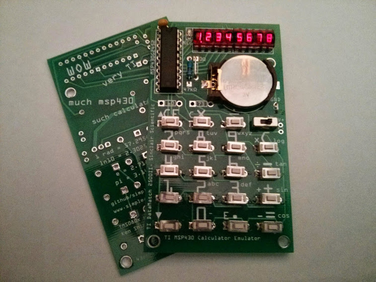
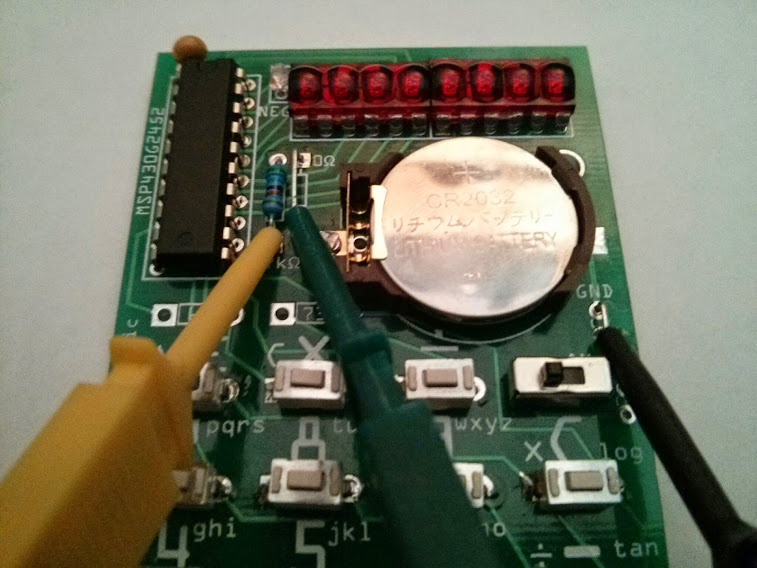
Here is a close-up and a hookup for in-circuit programming (via a G2 LaunchPad)
Parts / Bill of Material
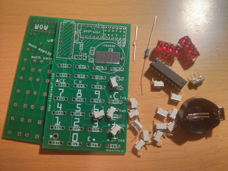
- 1 MSP430G2452, from your the Launchpad G2 (the "other" chip in the package), G2402, G2412 or G2432 will also work.
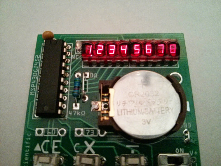
- 2 bubble led, from sparkfun ($2.95 ea)
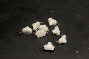
- 20 tactile buttons, 6 x 3 x 4.3mm, from DX ($4.76/100)
- 1 spdt dip size switch, from DX ($7.37/100)
- 1 CR2032 cell holder, from DX ($3.14/20)
- 1 miniature 1.8mm red led thru-hole, forgot where I got it (see picture)
- 1 47k pull-up resistor
- 1 0.1uF by-pass capacitor
The miniature red led is to show the "negative" sign. The original calculators have 9 digit displays, since we have only 8 digit, I used a led to show the negative sign when needed.
You can try different CR2032 cell holders, or even paper-clip diys, the pcb make provisions to mount different cell holders.
Schematic, Source Code and Build Hints
It is easier to understand the connections w/ the ascii art schematic, in my opinion
              MSP430G2452
            -----------------
        /|\|                 |
         | |                 |
         --|RST              |
           |                 |       2 x 4 digit bubble led
           |     digit 0 P2.0|----- +---------+ +---------+
           |     digit 1 P2.6|----- | % % % % | | % % % % |
           |     digit 2 P2.1|----- +---------+ +---------+
           |     digit 3 P2.2|--/-------+
           |     digit 4 P2.3|--/---|>--+ led (minus sign)
           |     digit 5 P2.7|--/-
           |     digit 6 P2.4|--/-
           |     digit 7 P2.5|--/-        segment a to g + dot........
           |                 |       /                                 ....\
           |                 |      /                                       \
           |   segment A P1.2|-----+-----+-----+-----+-----+-----+-----+-----+
           |                 | _=_ | _=_ | _=_ | _=_ | _=_ | _=_ | _=_ | _=_ |
           |   segment B P1.3|-o o-+-o o-+-o o-+-o o-+-o o-+-o o-+-o o-+-o o-+
           |                 | _=_ | _=_ | _=_ | _=_ | _=_ | _=_ | _=_ |
           |   segment c P1.7|-o o-+-o o-+-o o-+-o o-+-o o-+-o o-+-o o-+
           |                 | _=_ | _=_ | _=_ | _=_ | _=_ | _=_ |
           |   segment D P1.1|-o o-+-o o-+-o o-+-o o-+-o o-+-o o-+
           |                 | _=_ | _=_ | _=_ | _=_ | _=_ |
           |   segment E P1.5|-o o-+-o o-+-o o-+-o o-+-o o-+
           |                 | _=_ | _=_ | _=_ | _=_ |
           |   segment F P1.4|-o o-+-o o-+-o o-+-o o-+
           |                 | _=_ | _=_ | _=_ |
           |   segment G P1.0|-o o-+-o o-+-o o-+
           |                 | _=_ |
           |   segment H P1.6|-o o-+        (not all buttons populated)
           |                 |
            -----------------
The source code is in github
There is also good amount of H/W information commented inside the code
If you plan to design your own PCB, the basic principle in relationship w/ the code is
- P1 for LED segments
- P2 for LED digits
- P1 also for key button scanning
- You can move things around as long as you observe the above. I.e. If it fits better on your PCB, you could swap digit 1 w/ digit 3, segment A w/ segment E, etc, etc. All you need is to change #define in a header file and compile.
 Jeremy
 likeablob
 DIY GUY Chris
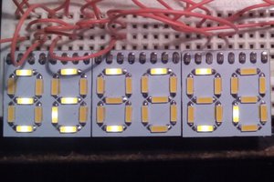
 Yann Guidon / YGDES