 Ced
CedThis project was triggered by the incredible set of videos from Ben Eater and James Bates. Many thanks to both of them.
I do not pretend to be an expert in computer hardware. As a professional in the software side of things, I wanted to learn more and build myself a working TTL based CPU to improve and try out ideas.
Even if this build is based on both Ben Eater and James Bates design, I wanted to really understand every bit of the design and therefore I have made many changes along the way. I do not pretend they are better, they are mainly driven by the fact of testing things (different choice in chips, different approach, try an learn).
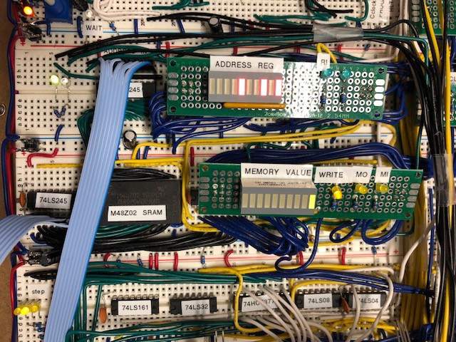
One thing that was really improved is the instruction set. The choice of having 8bit instructions and 256 bytes of memory really made it possible.
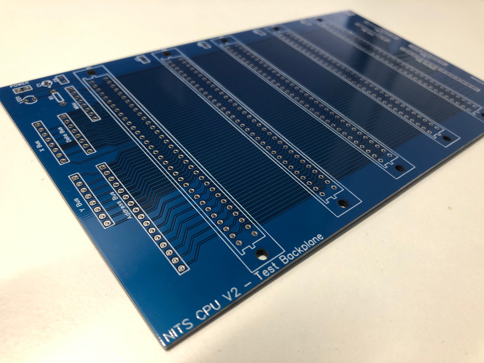
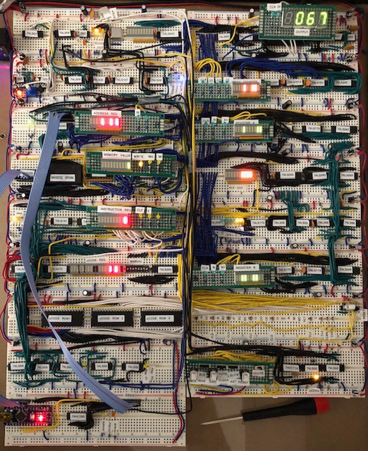
Once the Nits Processor was up and running, I started working on an improved V2.
These log posts are related to Nits V2:
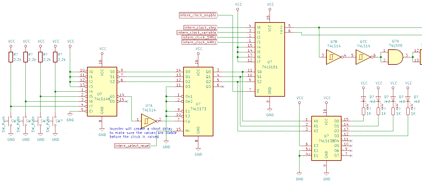
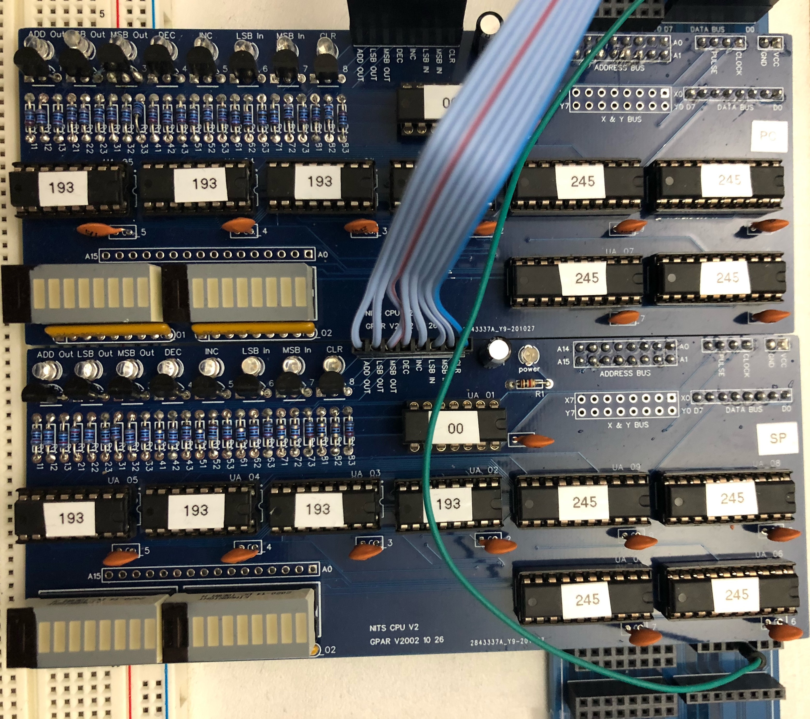
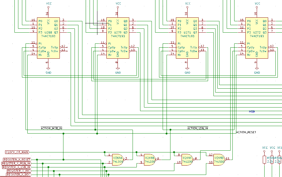
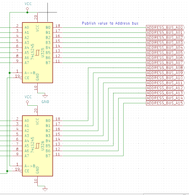
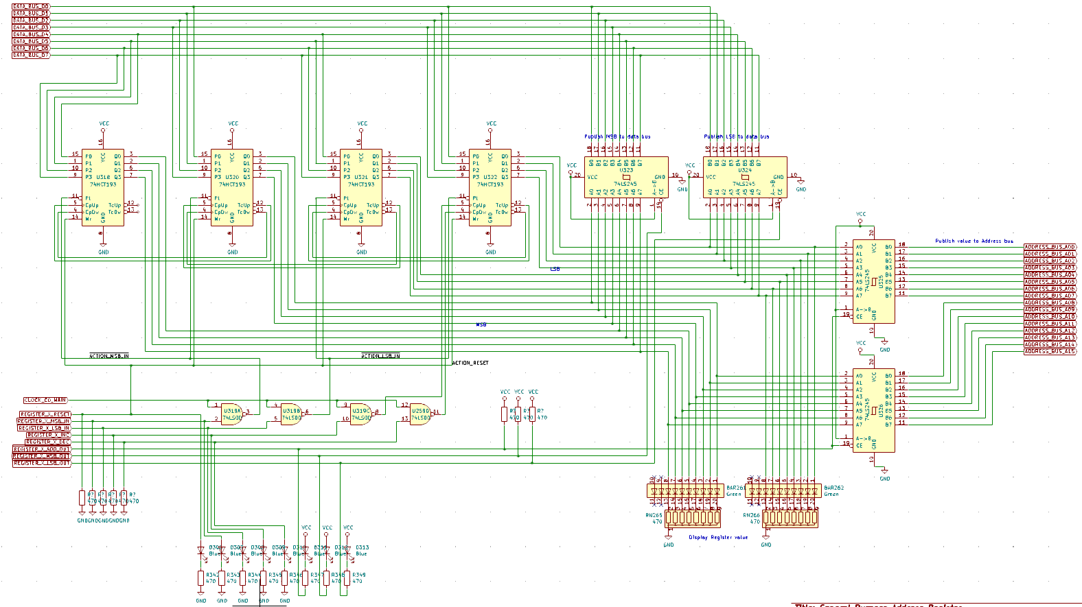
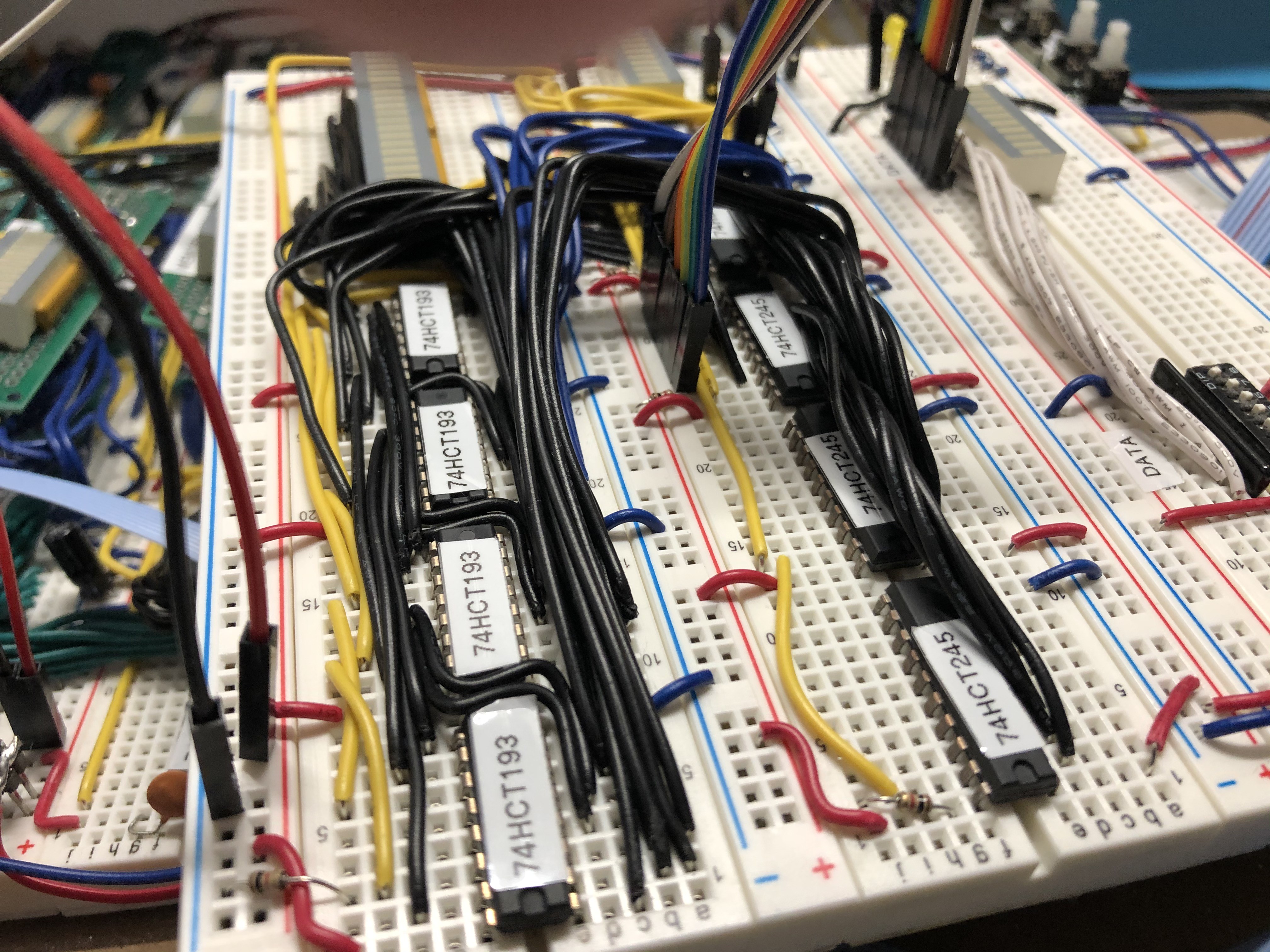
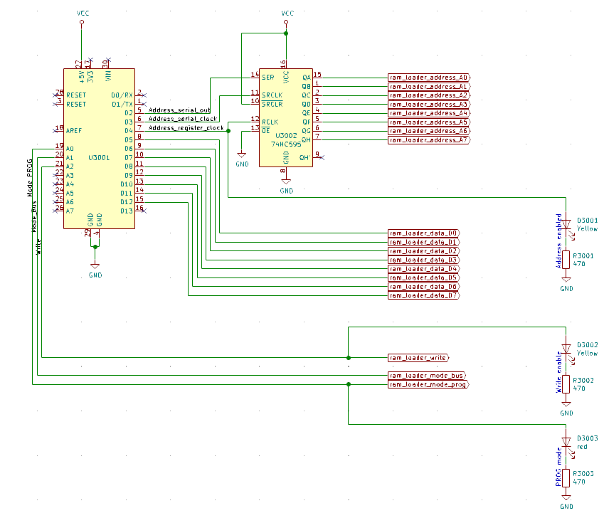
Prototype of the new Address Register
Testing the GPAR using an Arduino
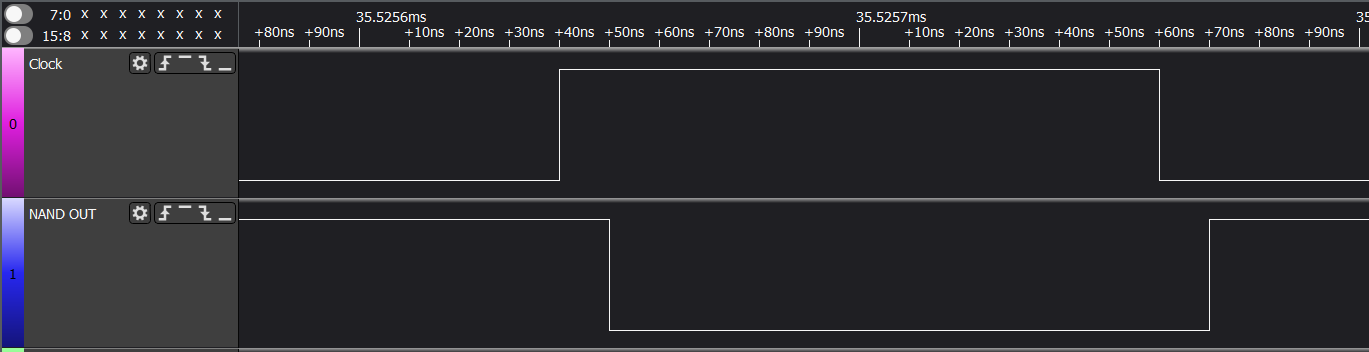
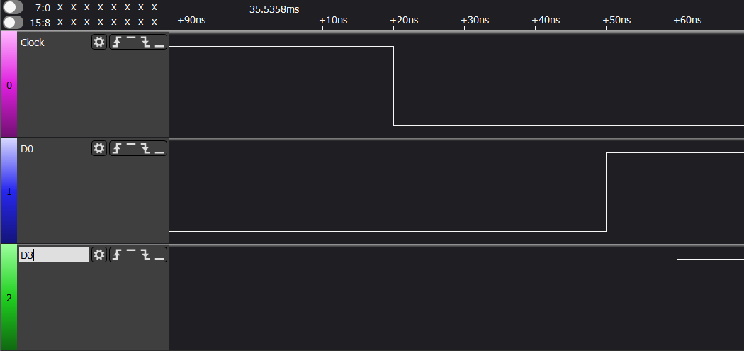
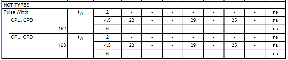
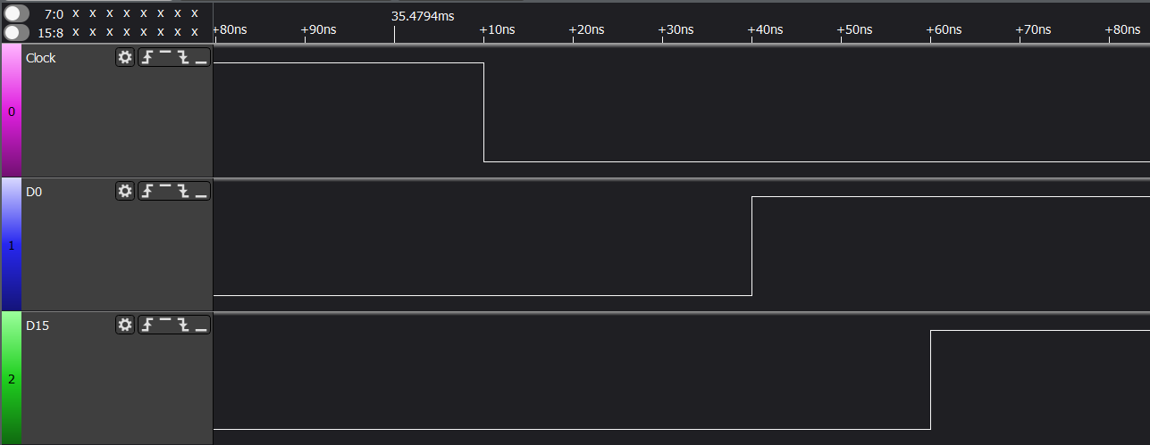
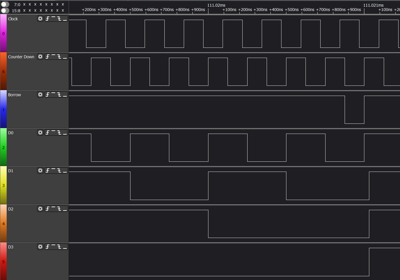
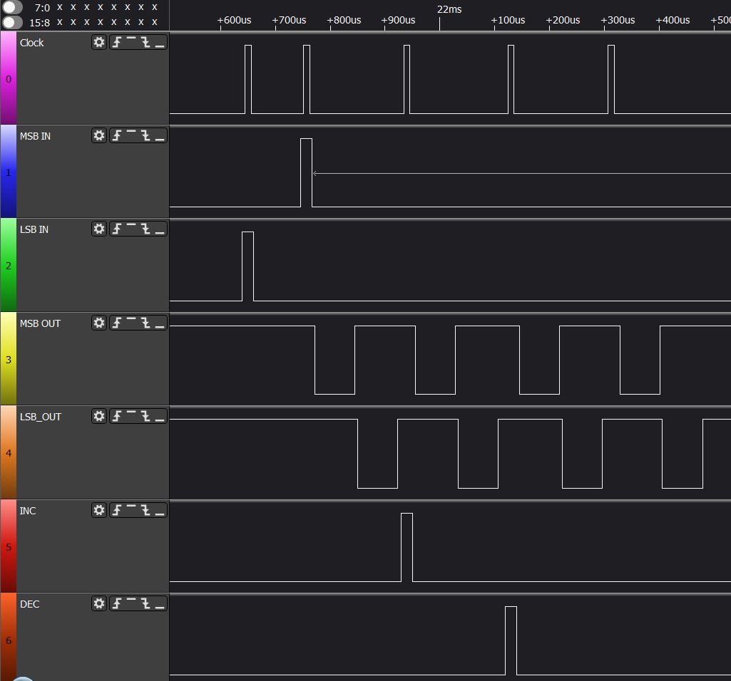
Measuring propagation delay and look-ahead signal
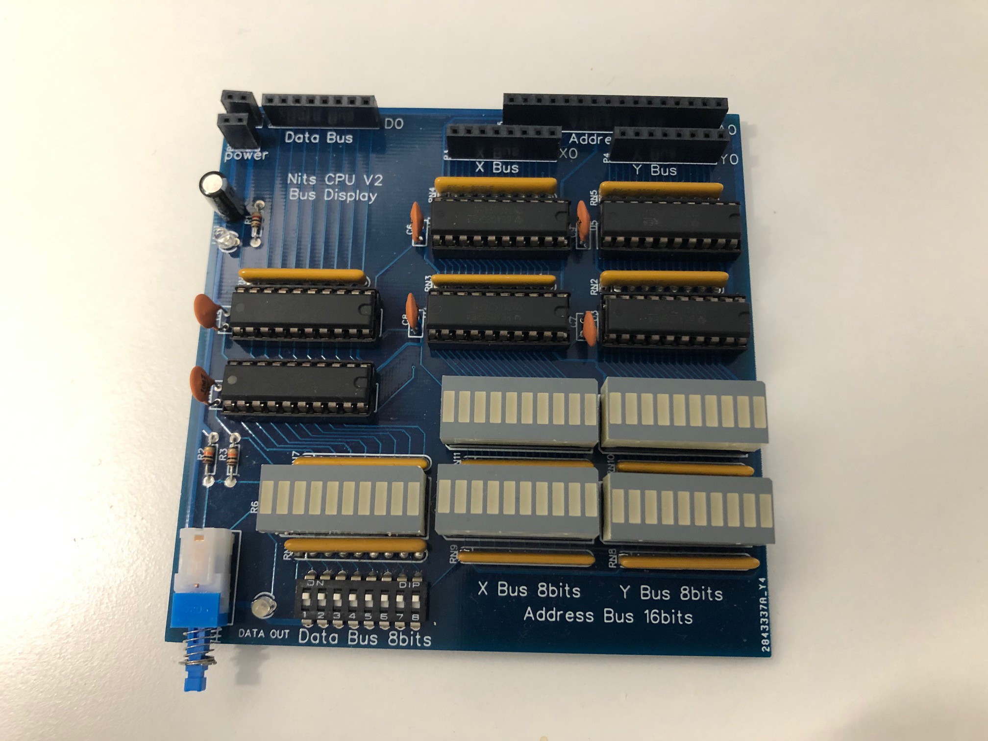
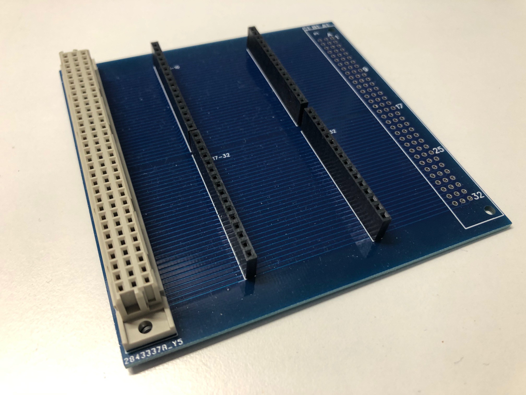
New PCBs for the Address Register
TTL Radio button for the Clock
and more to come...
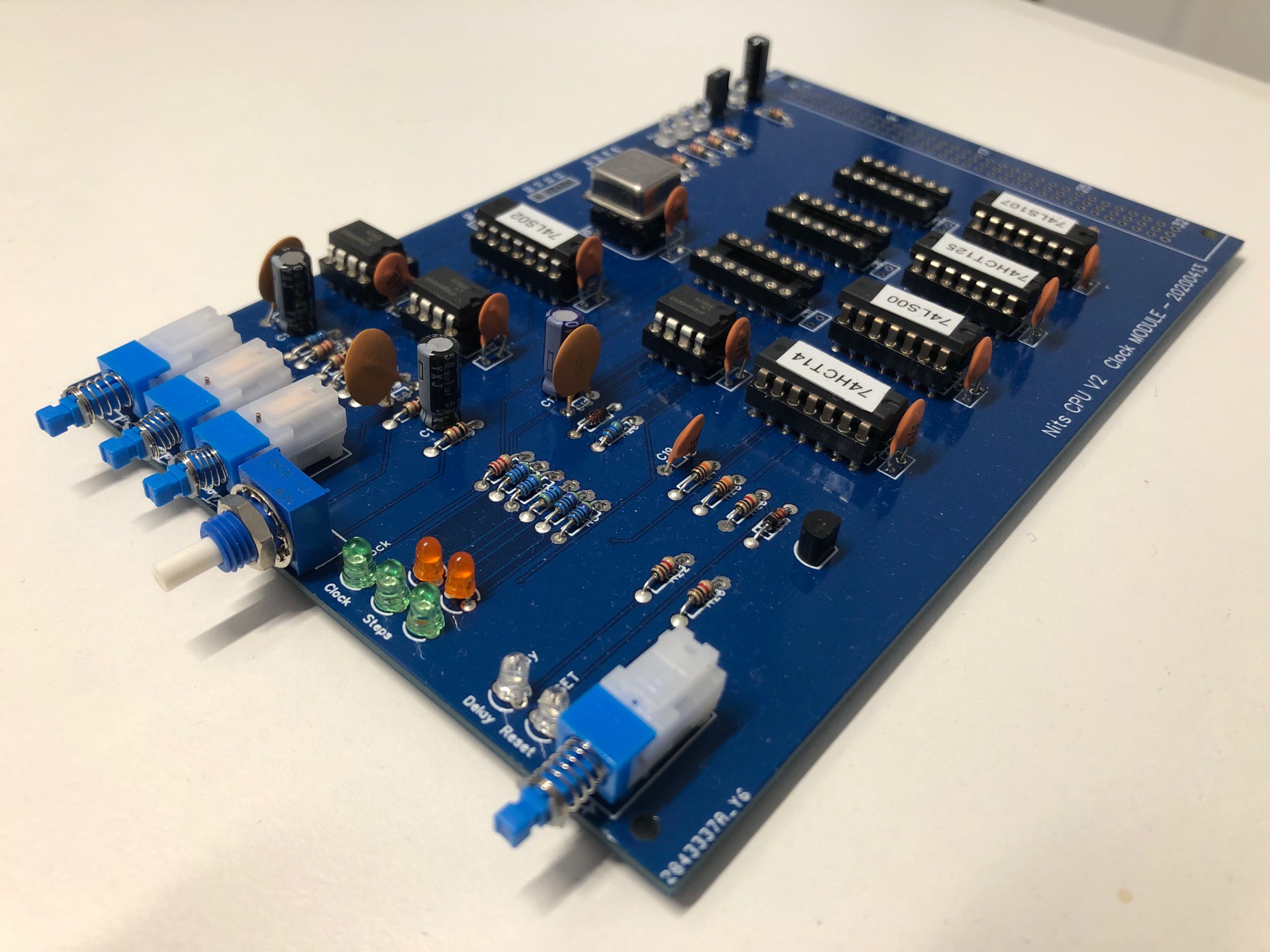
These log posts are related to Nits V1:
The clock Module (Clock part 1)
All about registers (Registers part 1)
Program Counter (Registers part 2)
Setting, Terminating, Displaying the bus
More about the clock (Clock part 2)
Selecting the right register IC (Registers part 3)


 Dave Collins
 agp.cooper
 jaromir.sukuba
 spudfishScott
Do you have any higher res images?
Looking to work on my own version!