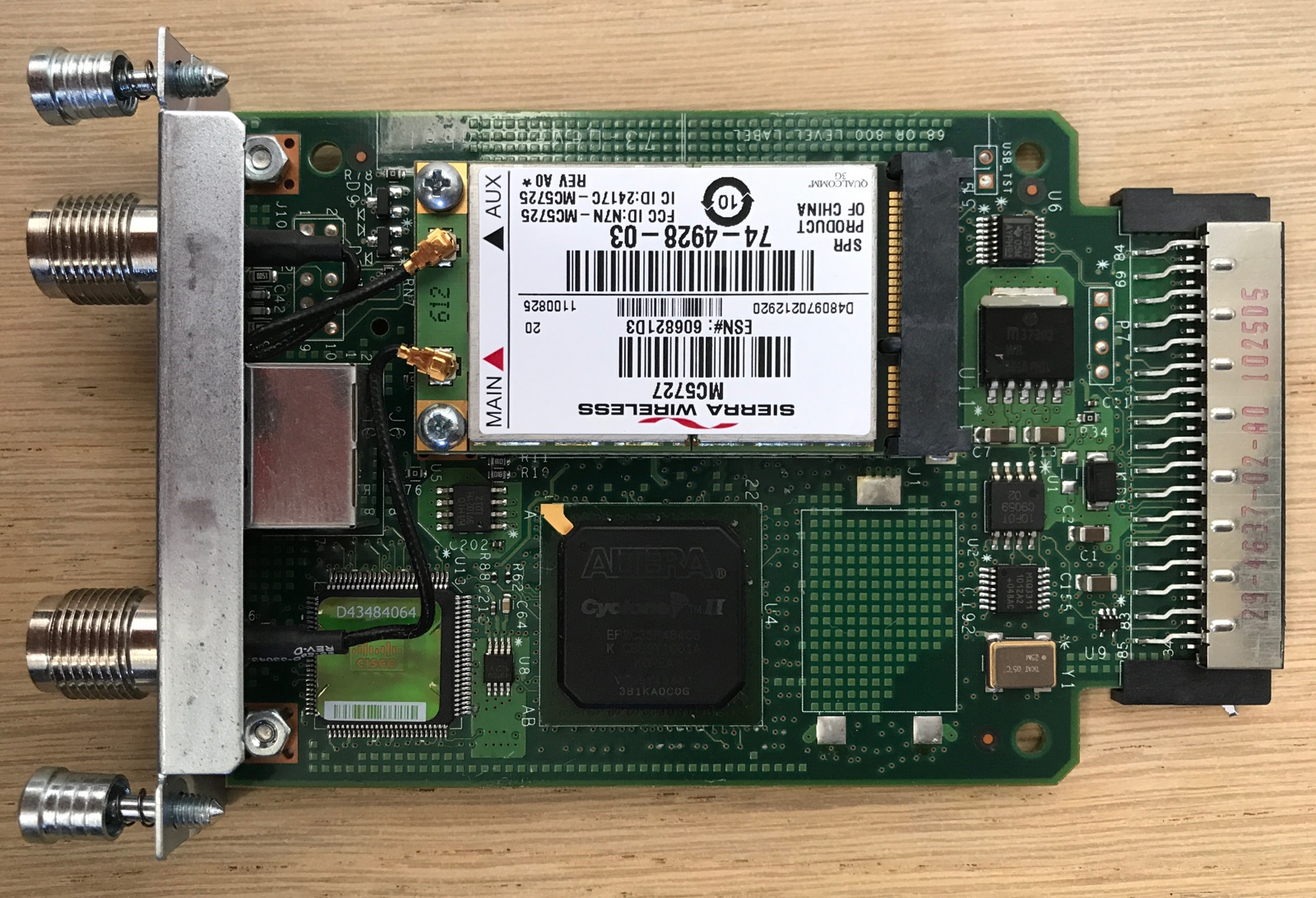
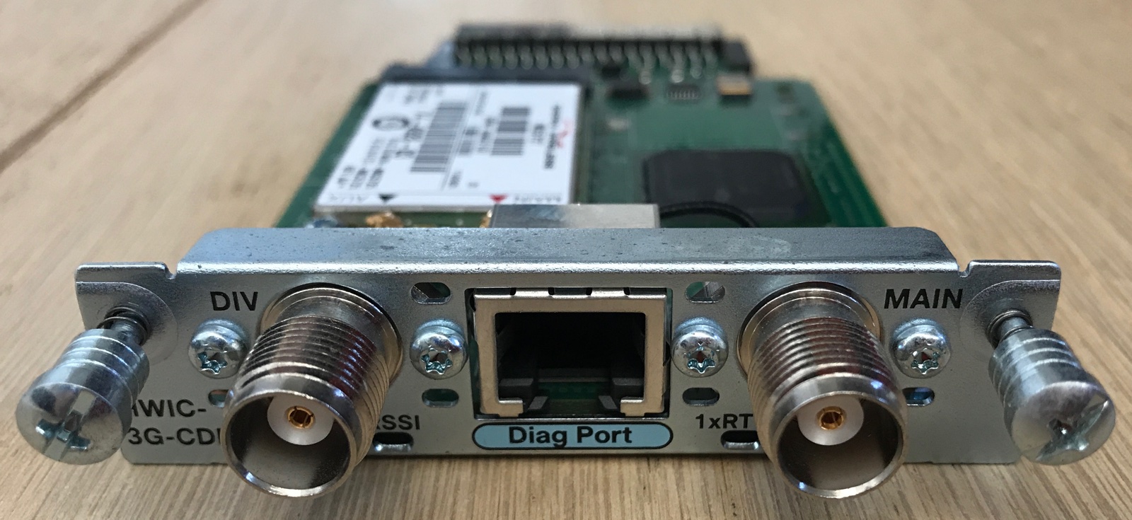
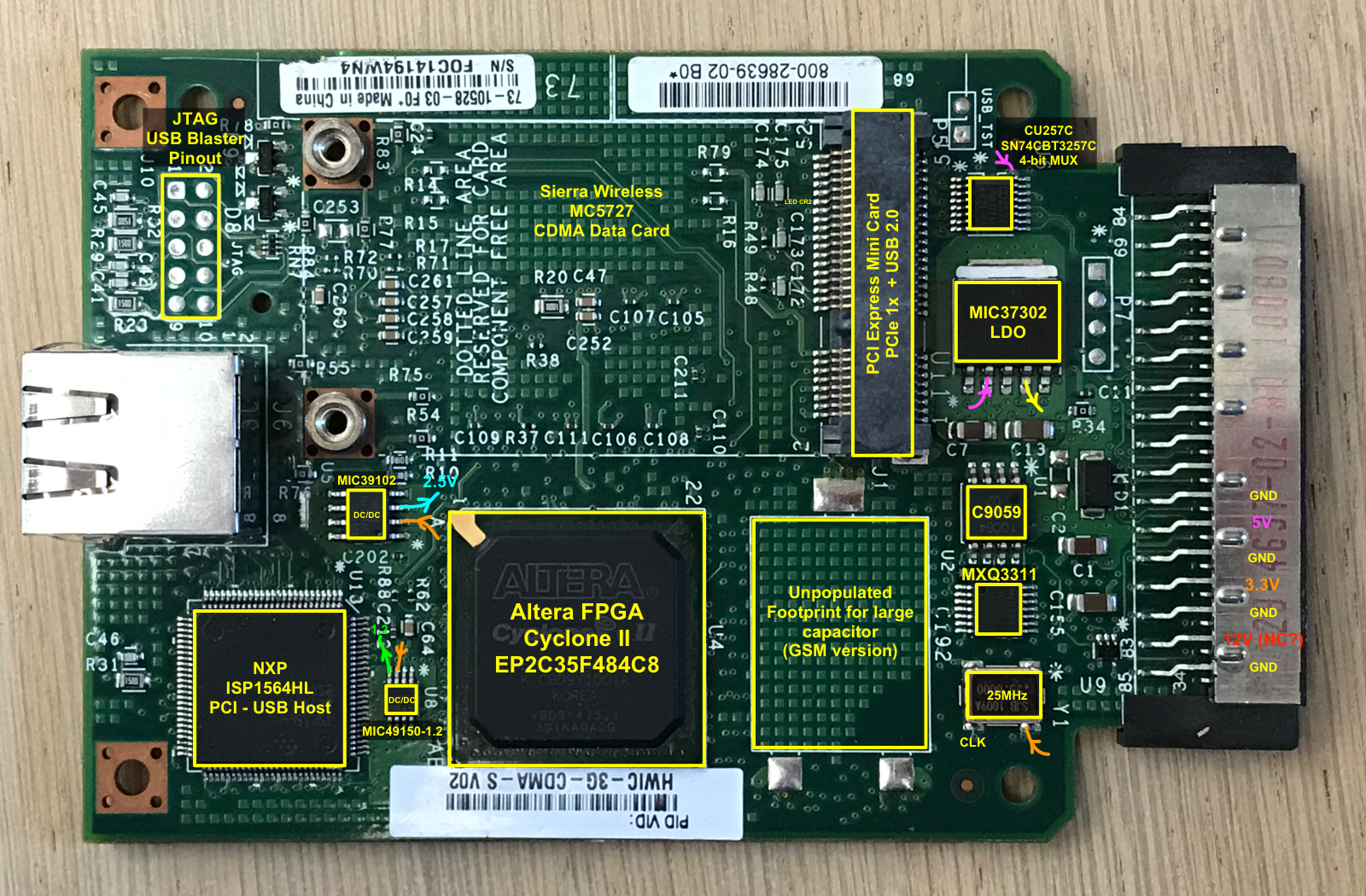
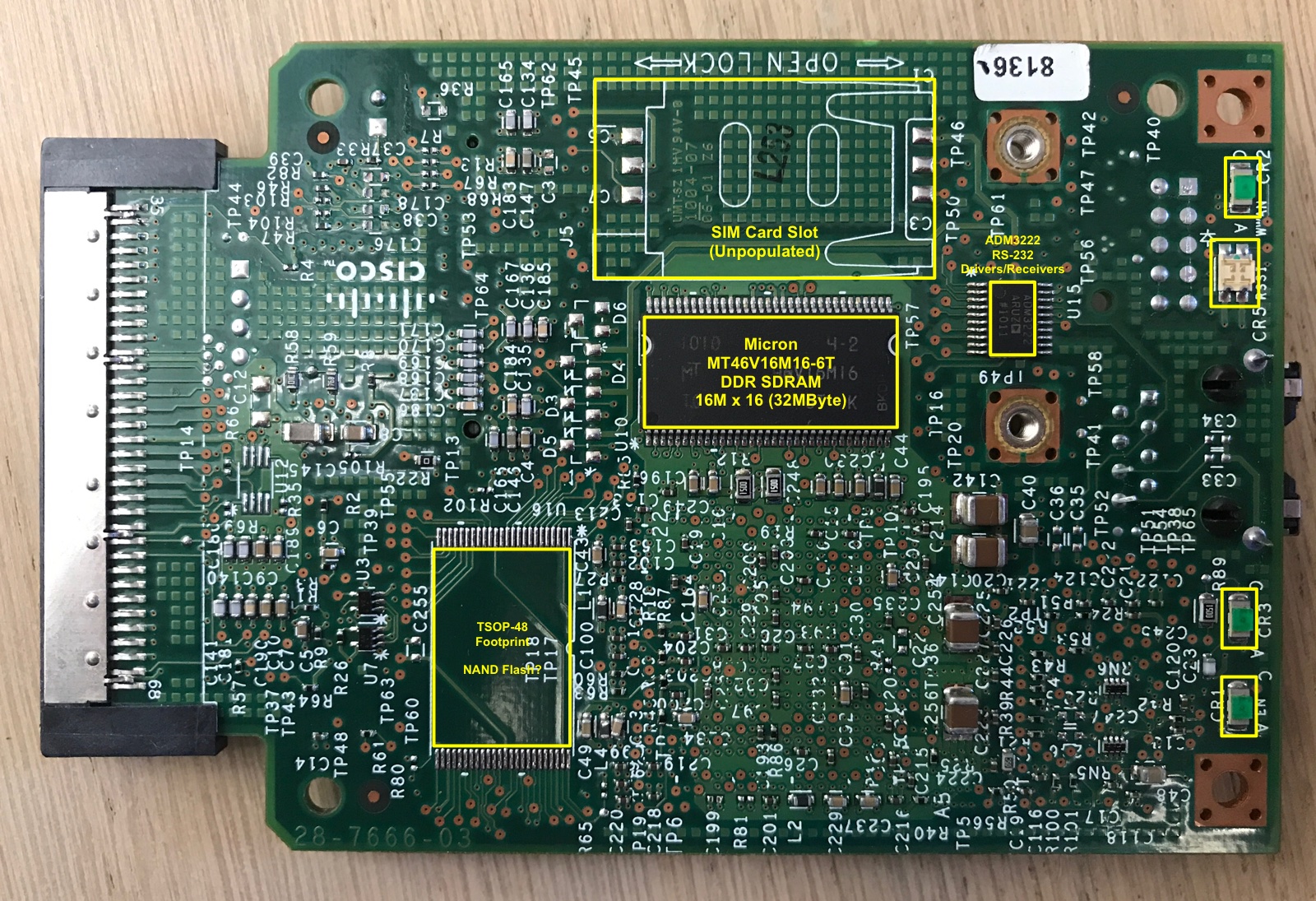
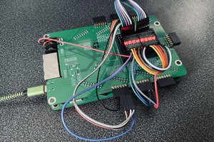
• Reverse Engineering the Cisco HWIC-3G-CDMA

    Tom Verbeure11/19/2019 at 06:49 1 comment

    (Originally published here.)

    The Cisco HWIC-3G-CDMA PCB

    After the abandoned attempt (*) to reverse engineer the $5 Cisco VWIC2-2MFT-T1/E1 card (because its Stratix II FPGA is not supported by Quartus Web Edition), I set my sights on another Cisco WAN card, the HWIC-3G-CDMA. This one has a Cyclone II EP2C35F484C8 instead of a Stratix II EP2S30F484C5N, and you better believe that I verified it being supported by the free Quartus version before starting this project!

    Cisco HWIC-3G-CDMA Top View

    This board is supposed to be inserted in the HWIC slot of a Cisco router and provide WAN functionality, allowing the router to link a local network to the world through a wireless (slow!) CDMA connection.

    Cisco HWIC-3G-CDMA Front View

    At the front, there are 2 antenna connectors and a diagnostic port. Don’t get too excited about the presence of an Ethernet interface: it’s an RJ-45 port that carries a serial interface using standard RS-232 voltage levels. USB-to-serial-RJ45 cables go for about $10 on Amazon, but they are not required if you have no need for a serial port.

    The Cisco marketing documentation mentions all kinds of protocols, but it’s safe to assume that no matter whether or not one of those supported protocols is still in active use, it’ll be very slow, and probably obsolete soon.

    At the time of writing this, the cheapest such cards could be bought on eBay for $8, including shipping. As usual, I started out by buying 2, allowing me to destroy one by desoldering components for easier tracing of connections.

    I’m not the first one to have a go at this board: the FPGA Board Hack project on Hackaday.io did some work on this as well, but other than a Quartus project on GitHub to blink the LEDs, nothing has been documented: no connections from FPGA to connector, no explanation about how to power the board etc.

    This is a pity, because this board has the promise of offering a pretty large, by hobby standards, FPGA with DRAM, for one of the lowest prices around! Let’s correct that!

    An Annotated Overview of the Board

    Cisco HWIC-3G-CDMA PCB Top Annotated

    Cisco HWIC-3G-CDMA PCB Bottom Annotated

    The PCB has a number of unpopulated component sites. That’s because the design is used not only for the CDMA version, but also GSM and HSPA variants, called, unsurprisingly, HWIC-3G-GSM and HWIC-3G-HSPA, both of which go for a considerably higher price on eBay.

    The GSM version has a standard full-size slot for a SIM card as well as a large capacitance that’s lacking on the CDMA version.

    On the back side of the PCB, there is an intruiging TSOP-48 footprint which isn’t populated for both versions. Was this originally designed to carry a flash chip?

    The core functionality of this board comes from an integrated Sierra Wireless module that slots into a PCI Express Mini Card.

    Note: the wireless module is held onto the board by 2 screws that were very tight, but used a weak metal. Both screws stripped when trying to remove them, and I had to use a special screw removal drill bit to get rid of them!

    Other than the wireless module, there’s the Cyclone II FPGA, and an NXP ISP1564HL USB 2.0 Host PCI controller. (Yes, that’s old school PCI, not PCIe!)

    This made me scramble to Google: why in the world would you need USB on a device like this?

    Turns out: a PCI Express Mini Card has support for 2 communication protocols between host and card: either PCIe 1x or USB 2.0. The more you know! Since this is custom solution designed specifically for the Sierra Wireless module, the Cisco engineers rightfully didn’t bother to wire up the PCIe interface signals.

    Also present: a 32MB DDR SDRAM for all your volatile data storage needs (yay!), and the usual supporting cast of voltage controllers, level shifters, LEDs, connectors, and various unknowns.

    Powering Up the Board

    The first step of reverse engineering the VWIC2-2MFT-T1/E1 card consisted of unraveling its power supply architecture. That board uses the full spectrum of available power sources of the HWIC connector: 12V, 5V and 3.3V (though you cheat your...

    Read more »