 Rory
RoryFeatures
- 3-12 cell voltage monitoring (external slave boards via CAN Bus)
- 12 NTC temp sensor inputs
- Cell balancing
- Isolated CAN Bus
- UART via Bluetooth
- Current monitoring via external hall effect sensor
- Ability to drive a MOSFET array or IGBT for discharge control
- Hard wired safety chain between boards
- Output for charge enable MOSFET
- Wake up function via button or external input
- Low standby current
- Infineon XMC1400 series micro
- Associated MOSFET board
Cell Monitoring
3 - 12 cells can be monitored. If less than 12 cells are motored solder bridges must be shorted to link the highest cell up to the highest input. For example, if 10 cells are monitored, solder bridges between cell 10, 11 & 12 must be shorted. A MAX14920 is used to simplify sampling of the cell voltages.
Temperature Sensor Inputs
12 inputs are provided to connect 10K NTC temperature sensors. This is to allow temperature monitoring of each cell parallel group.
Cell Balancing
The MAX14920 can enable balancing resistors on the PCB with a 100mA balancing current (may require additional heat sink)
Isolated CAN Bus
Isolated CAN Bus allows additional BMS boards to monitor additional cells as part of a high voltage pack
UART via Bluetooth
Board is designed to accommodate generic Bluetooth serial modules via a pin header.
Current monitoring
A 5V supply and analogue input provided for an external hall effect current sensor
MOSFET array or IGBT Driver
12V drive with 6A peak current for discharge control
Hard wired safety chain between boards
Board requires a 12VDC power supply to enable the discharge MOSFET/IGBT. In and out connectors are provided to chain to other boards. The master BMS can be configured to send this signal to slave devices. Can be wired from an external emergency stop signal to disable battery independently of the CAN Bus. Can be disabled with 0 ohm resistors.
Output for charge enable MOSFET
5V logic output to dive a charge enable MOSFET
Wake up function via button or external input
A tact button is provided on the PCB to provide a wake up function from low power mode. This is also linked to a pin header with a 5V switched supply for an external illuminated button
Low Standby Current
VCC to temp sensors, current sensor, Bluetooth etc are all seperately enabled by P channel MOSFETS to keep running current to a minimum. Minimum sleep current TBC
Associated MOSFET Board
An associated board with matching dimensions and mounting holes can be connected below the BMS via a pin header. Has room for 6 paralel D2PAK-7PIN MOSFETS as well as 2 x TO-252 MOSFETS for charge control.
PCB Layout Notes
As my other projects, all components are on one side of the board to allow easy SMT soldering via a hot plate. Board is 2 layer to take advantage of cheep board houses. This made layout very challenging. I will go 4 layer next time I think...
Firmware Progress
Development has not begun due to buying a house that needed much work... Will pick this up again soon!
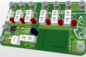
 McGill Formula Electric
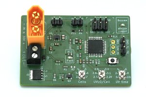
 Jan
Jan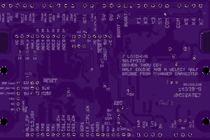
 ronald.sutherland
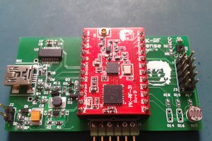
 peritronics