 MagicWolfi
Just like everybody else, the chip shortage has caught up to me sooner or later. The controller chip CYPD3177 for my USB-C Power delivery (PD) sink was out of stock everywhere for several months. So I decided to order boards populated with everything except the chip (and some of them also without the switches as they were short on stock as well). Sometimes the quick turn assembly houses only stencils solder paste onto the pads of the populated components, no matter what the provided Gerber paste layer looks like. With this in mind I tried to come up with a new (for me) method to apply paste for re-flowing the chip.
When the IC was available again I bought enough to finish all the boards and put them in stock in my Tindie store.
Enter the "selective solder stencil". I created a new paste layer and left only the chip pattern as intended to have the pin pads and the bottom center pad open. For all other components I created openings as big as the perimeter of component body+ solder pads. This enables the stencil to slide over already populated components and as a nice side effect being perfectly centered over the empty footprint. I ordered the stencil from OshStencils, as Polyimide film. A thin strip of cut credit card served as paste squeegee to spread the paste only in the desired area. Lifting the stencil left the paste in the correct place. The distribution was not perfect due to the fact that the polyimide stencil was not perfectly flat but bowing up a little. But during re-flow/hot air soldering, the solder usually knows where to go to build nice solder joints and no bridges.
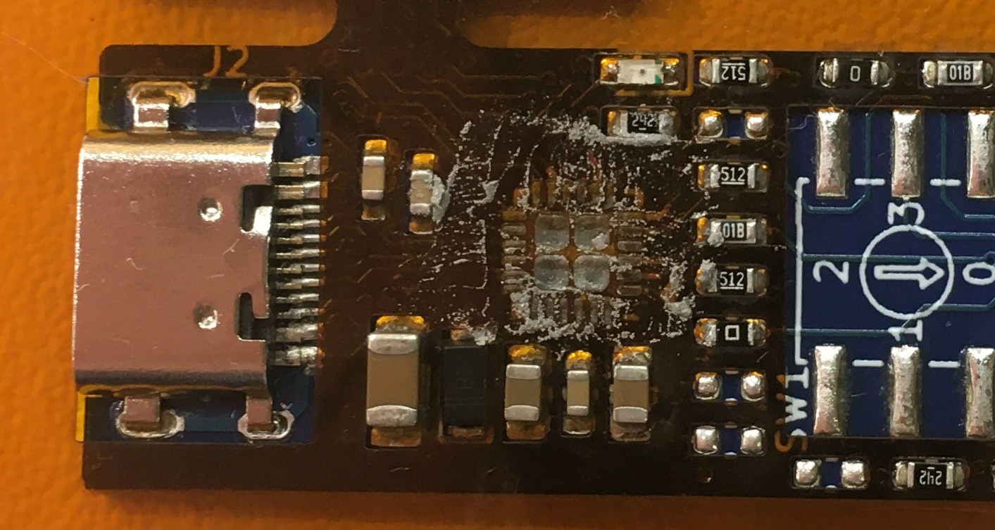
For this try I used hot air for soldering as the screw terminal would not be happy about excessive time on the hot plate. Everything went smooth and the board worked perfectly as expected.
This exercise remained a proof of concept, as the board house was so kind to also put solder on the un-populated pads, which made the whole process easier. Putting down some sticky flux was enough to activate the existing solder and connect the chip just as good as with fresh paste. Next time I would make the opening maybe 1 or 2 mil (25 um or 50 um) wider to give some tolerance to the whole process.
Here are some pictures to demonstrate the steps from empty board to finished assembly:
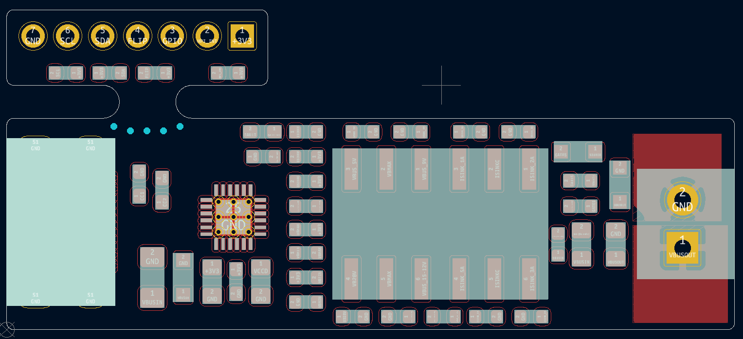
This is how the KiCAD design looks like; light blue is the selective solder stencil layer with the red pads shining through.
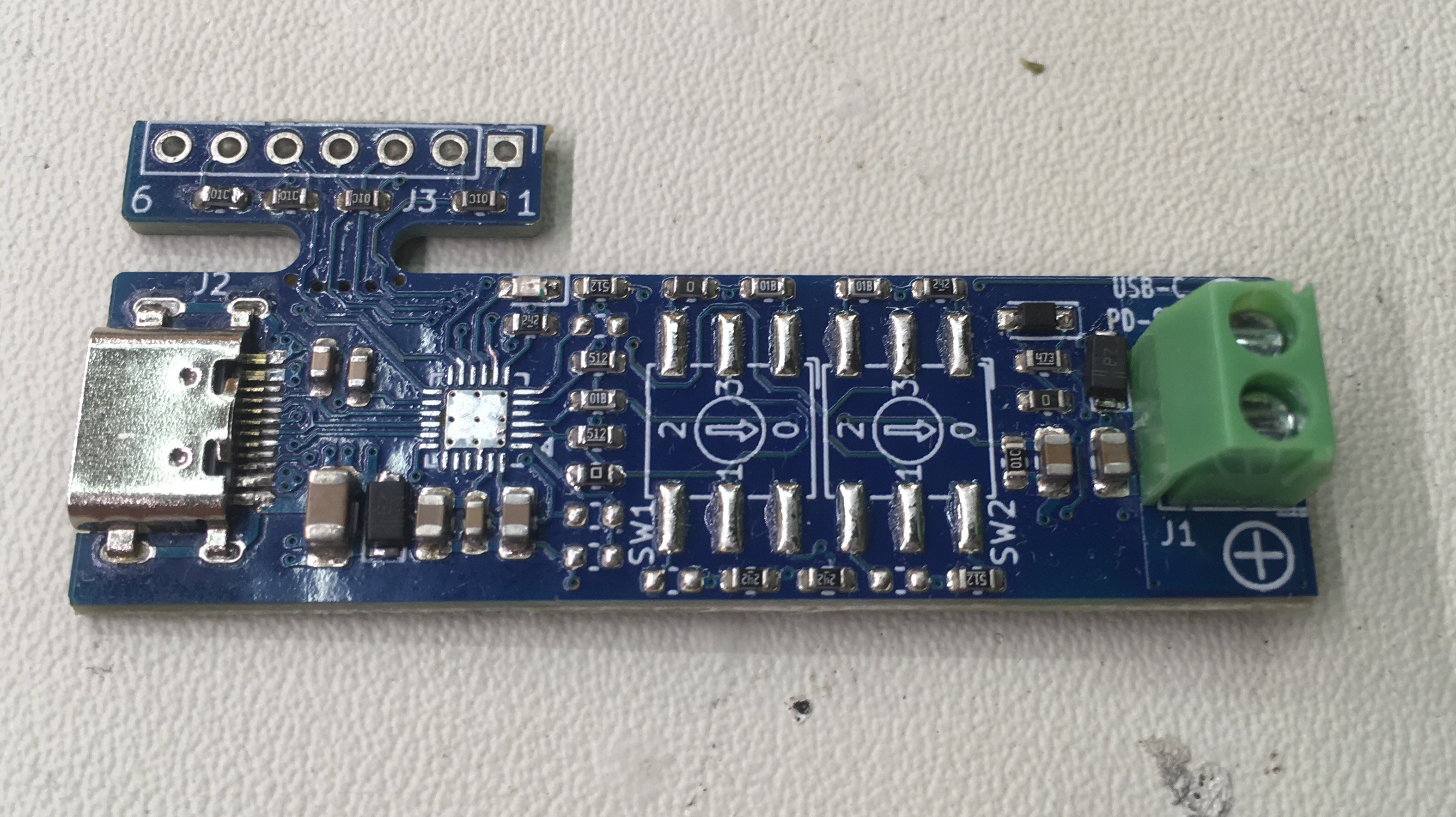
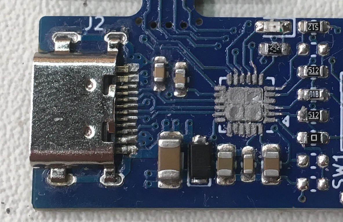
The partly assembled board with a clean footprint for the chip to be populated
The orange stencil placed over the board. The already assembled components are sticking nicely through the openings. A somewhat enough amount of paste is ready to be spread over the footprint.
Solder is squeezed into the stencil openings.
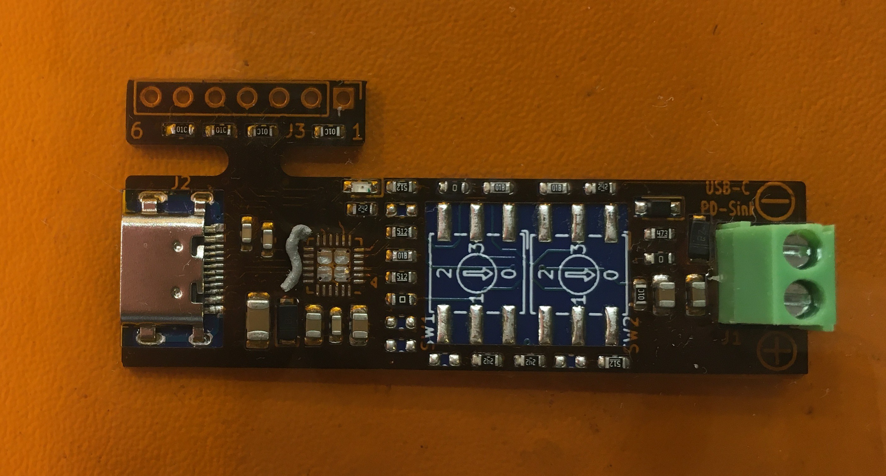
The pasted board without the stencil ready to have the chip placed onto the pads.
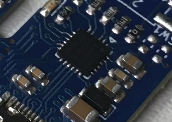
And the finished board:
Discussions
Become a Hackaday.io Member
Create an account to leave a comment. Already have an account? Log In.