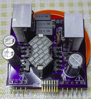
The charging section and basic backplane design are finally done. The SEPIC card went thru a few iterations to get ringing in the switch & rectifier under control. A tight PCB layout is critical which includes keeping the outbound & return power traces aligned. Interestingly, I tried a synchronous rectifier but the efficiency gains were negated by the excessive snubber losses: the gate charge exacerbated the main switch turn-off ring due to inductive layout parasitics between the coupled inductor / coupling capacitors and the synchronous switch. Reverting to a schottky rectifier allowed for a much tighter layout that eliminated most of the ring and allowed the use of a small snubber. Now the switch runs hotter than the rectifier - goes to show that simpler is often better.
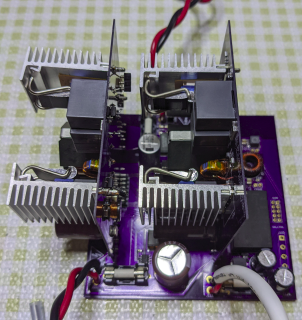
Here's the current build. The backplane contains the master controller for both SEPIC cards, +5V & +12V bias supplies, connections for PV (charger) in, battery stack (charger) out, and the balance bus battery.
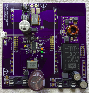
Each SEPIC card mounts vertically via a set of soldered pins that provide mechanical support. The charger in/out sections include LC filters and hall effect current sensors to support MPPT and managing the stack's charge state.
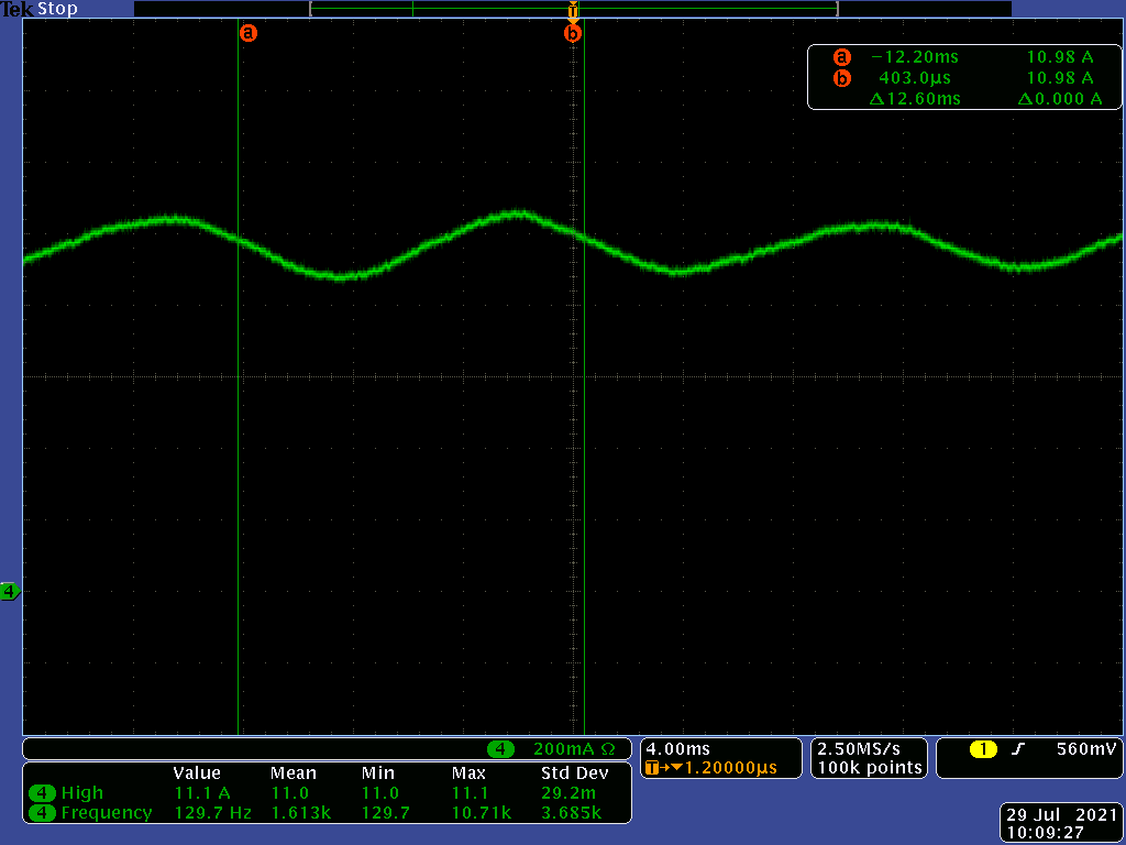
Input Ripple Current
As discussed in prior logs, the SEPIC topology was selected in part due to the input current being continuous and the ability to 'steer' ripple current to the output with the use of a coupled inductor. The worst-case line & load condition is Vin=10V & Pout=90W. The trace below shows ~ 200mA P-P @ ~ 130Hz. Not bad.
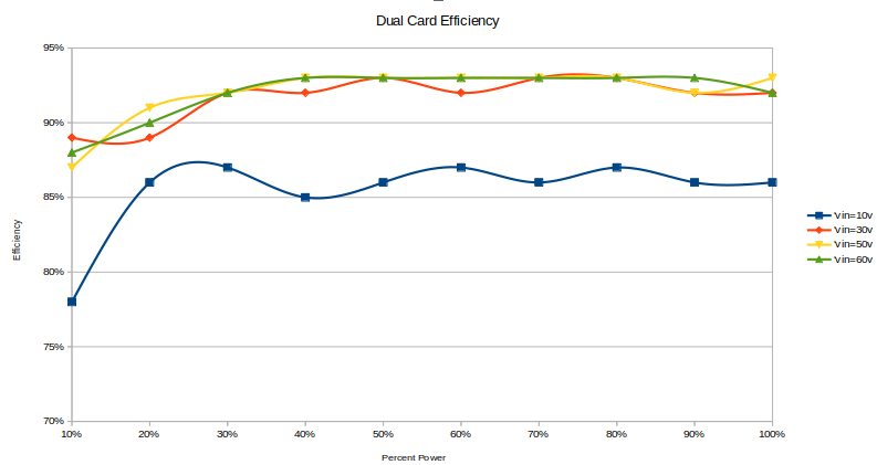
Efficiency
The design derates the charger's output as a function of Vin.
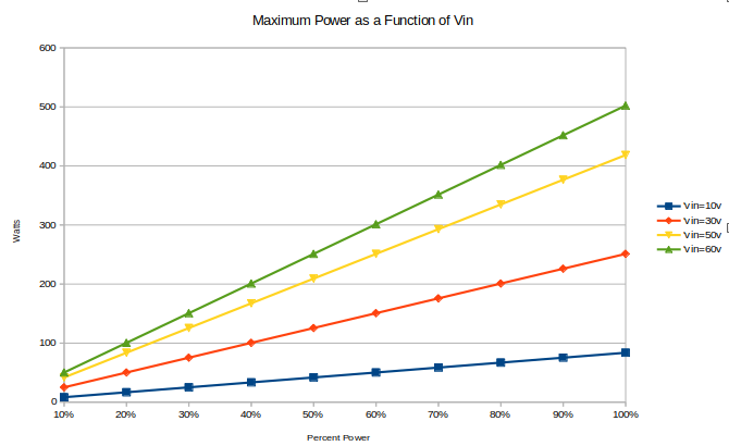
This maintains a relatively constant [maximum] input current to match the power curve of the PV array. Efficiency was measured with both cards operating at four input voltages. Minimum Vin, 10V, is the worst but at 30V & above the curves are surprisingly close with efficiency peaking at about 94%.
Next Up
The charge balancer section isn't ready yet but the backplane includes the necessary connections (right edge of backplane) for a development version. Once that's done the backplane will be redesigned to either support the balancer as a card or integrated. The SEPIC cards will undergo a final design revision to accommodate changes to the pin configuration on the backplane and to move temperature sensing from the rectifier to the switch.
Thermal management will also drive the final layout. Natural convection was the original design goal (hence the vertical cards & heatsink fin orientation) but that is not realistic. Forced convection will likely dictate that the assembly rotate 90 degrees so that the SEPIC cards are horizontal and the fan can exhaust out the side of the enclosure.
Discussions
Become a Hackaday.io Member
Create an account to leave a comment. Already have an account? Log In.