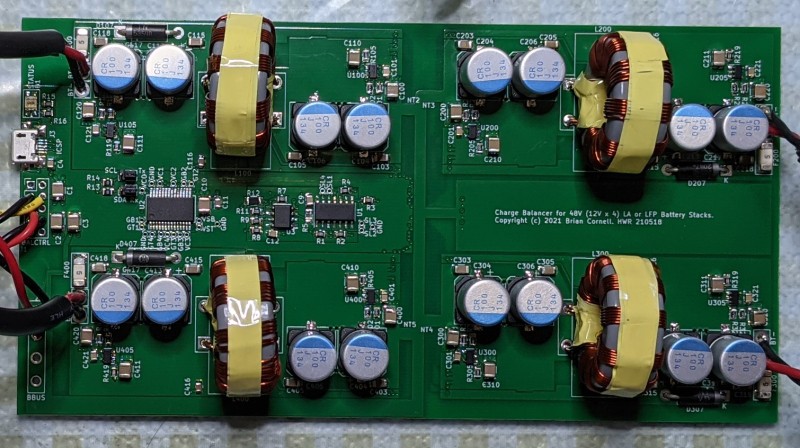
The Battery Balancer is the final module to complete the PV->Battery charger design. It adheres to the original proof of concept and uses individual, bidirectional flybacks, to both transfer charge and measure battery voltage.
Specifications:
- Battery stack size: 12V x 4 = 48V (nominal, range 40V ~ 56V)
- Battery chemistries: Lead Acid (LA), Lithium Iron Phosphate (LFP)
- Architecture: per-battery bidirectional flybacks
- Operating frequency: 100kHz
- Voltage sense: via flyback voltage impressed on coupled winding
- Balancing method: timed direct transfer between highest & lowest batteries in stack
- Balancing resolution: 50mV
- Balancing current: ~1.5A (18W)
- Charge transfer efficiency: 77%
- Bias supply: +12V, +5V (provided by charger)
- Operating temperature: -20 - +50C
- Cooling: natural convection
- Calibration data and configurable operating parameters are stored in NVM
It integrates with the Charging module back plane for bias power and console access & control via 400kHz I2C.
Results are mixed. It does work as designed but in practice the combination of methodology and hardware selection is problematic. This is detailed in a subsequent log discussing performance & problems.
THEORY OF OPERATION
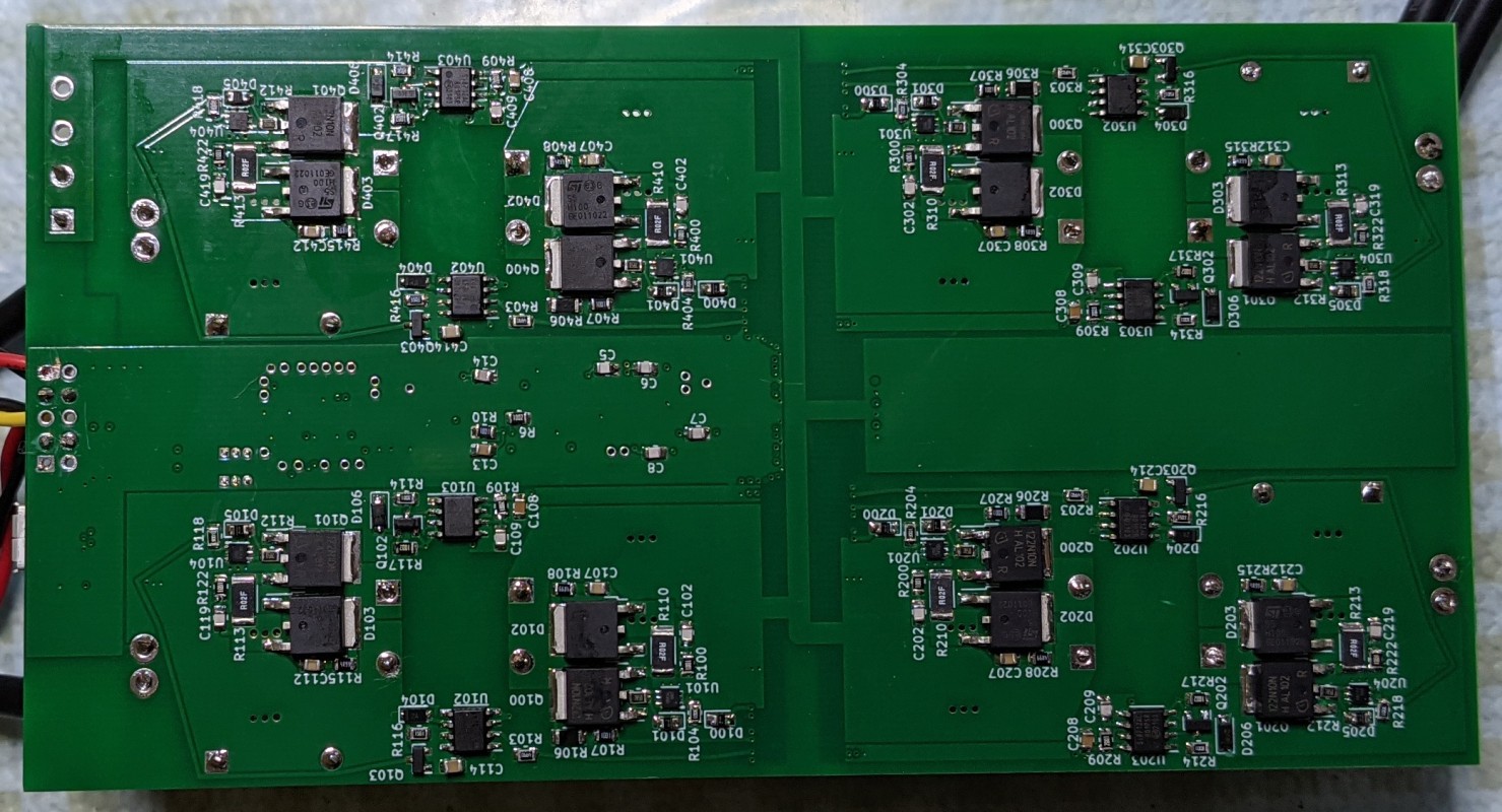
The Balancer consists of four identical bidirectional flyback sections, one per battery. The flyback inductor uses a 1:1 bifilar wound coupled winding that isolates the balancer from each battery and the common mode voltage of the stack. The balancer side of the flybacks connect to the balance bus which facilitates charge transfer between the batteries. It also connects the balance bus battery which powers the bias supplies and serves as a charge transfer buffer.
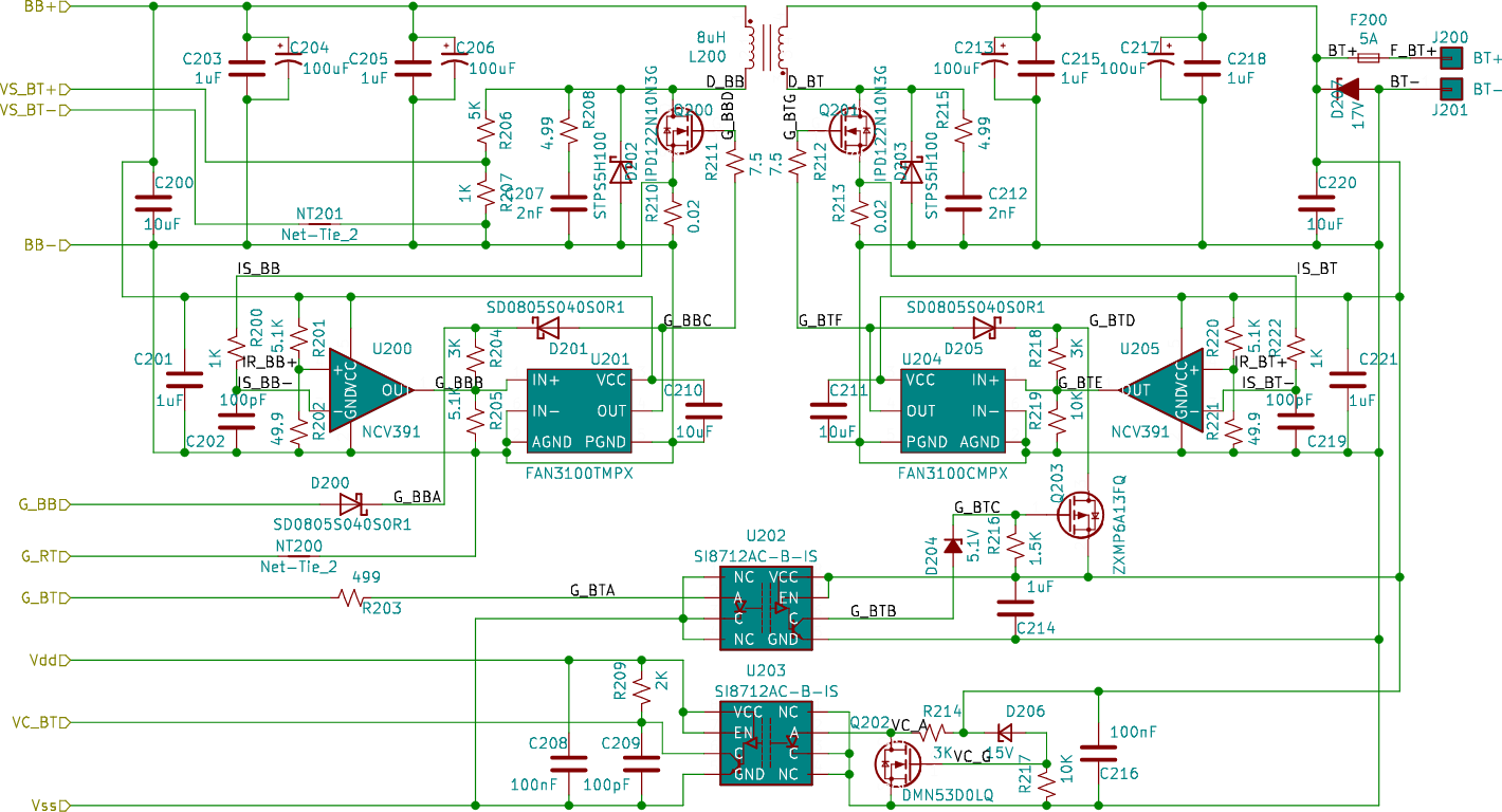
Each side of the flyback contains a low-side gate drive with the battery side employing an isolator for the gate drive signal. The gate drivers employ positive feedback via a schottky diode across the output/input to maintain the gate drive after a short (500nS) pulse from the controller to initiate the period.
The flyback control loop is 'constant on time': a low-side current sense resistor provides a voltage proportional to the inductor current ramp and is sampled by a comparator that terminates the duty cycle. The comparator's voltage reference is connected to the same supply as the flyback (e.g. either the battery or balance bus) which makes the flyback on-time ratiometric to the supply voltage and keeps power delivery consistent over a range of voltages. A schottky diode conducts the free-wheeling current.
This design is simple and rugged but must have a low impedance load (e.g. battery) connected to the output to avoid self-destruction. Since this cannot be assumed a protection circuit applies a logic high signal to the controller whenever the battery voltage is outside of safe limits (this is defined as a 'voltage condition' event). This signal is routed to the controller COG peripheral which terminates the gate drive without firmware intervention. The combination of bulk capacitance and a zener diode across the battery shunts excess energy for the few cycles required for the gate drive to terminate. In the event of controller failure the zener diode acts as a shunt to open the fuse and disconnect the battery. The controller incorporates a similar protection feature using a comparator, but this version of the design does not incorporate external shunt protection.
The battery voltage condition signals are OR'd, and the resulting logic signal is inverted and routed to the charger's controller via a dedicated pin. This allows the charger to immediately stop charging the stack. All of this occurs independent of I2C communication and without firmware intervention. Note that the balance bus voltage condition is not routed to the charger since it offers no additional protection or safety.
The Balance Bus flyback circuits contains precision voltage dividers that are used to sense the voltage impressed upon the gate drive during the battery flyback charge cycle. This voltage is the sum of the balance bus and battery voltage, (minus errors in inductor coupling, switch & current sense losses, etc.) and is routed to the controller section for measurement of the battery voltage.
An analog switch functions as a multiplexer to route the selected sense signal to a buffer & differential applifier. The differential amp subtracts the balance bus voltage and the controller's ADC quantitizes this sampled signal at approximately the midpoint of the flyback signal. Several samples are recorded & processed to derive the battery's voltage. This is more fully explained in the firmware code documentation.
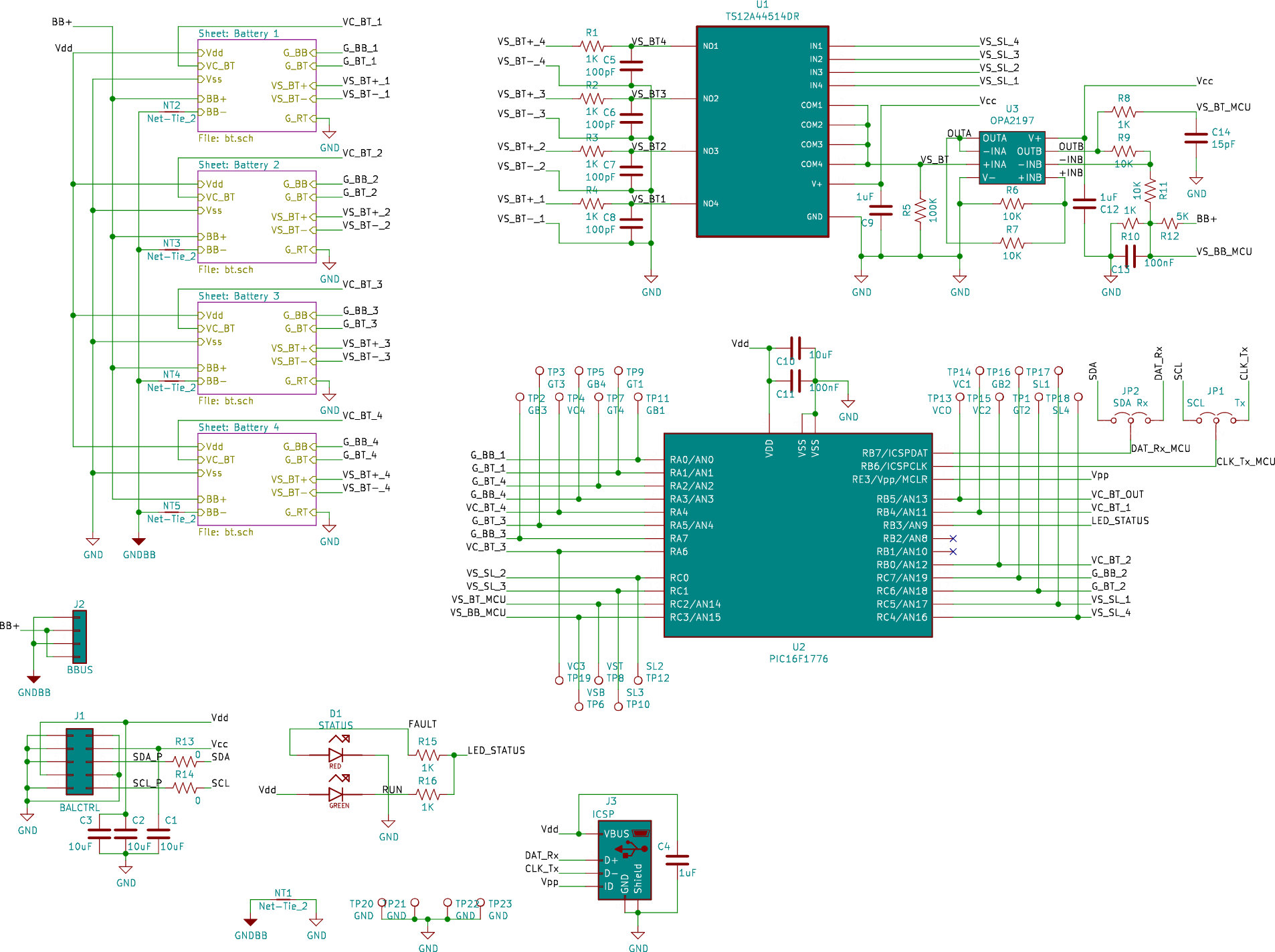
The controller is a Microchip PIC 8-bit mid-range 16F1776 running at 4 MIPS that controls the balancer and communicates with either a console via RS232 (stand-alone operation) or I2C connection to the charger (integrated operation). The operating mode is set by a compile option and on-board jumpers connect the common communication pins to either the micro-USB jack (RS232) or the I2C bus. A combination Red/Green LED indicates the Balancer's status: Green=normal, Red=fault. Some faults are treated as recoverable (e.g. the controller monitors for the condition to clear & resumes normal operation), and others require a power cycle or reboot.
The controller monitors the balance bus & battery stack voltages at regular intervals and when the difference between the highest & lowest batteries (or the balance bus battery becomes low) charge is transferred. Charge transfers run for specific, configurable, time intervals that are set based on the size of the batteries in use. Battery voltages are monitored during transfers to terminate if low/high safety limits are exceeded. Transfers always operate in pairs and 180 degrees out of phase: the flyback portion (discharge into the balance bus) of the high battery occurs during the charge portion of the low battery.
The controller uses NVM to record a number of operating statistics on the balancer's operation and each battery. These can be used to tune operation and identify a problematic battery. NVM is also used to store calibration constants and a variety of operating parameters. Refer to the firmware documentation for a detailed explanation of the controller's operation.
Discussions
Become a Hackaday.io Member
Create an account to leave a comment. Already have an account? Log In.