0%
0%
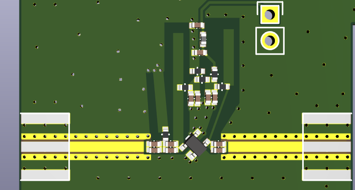
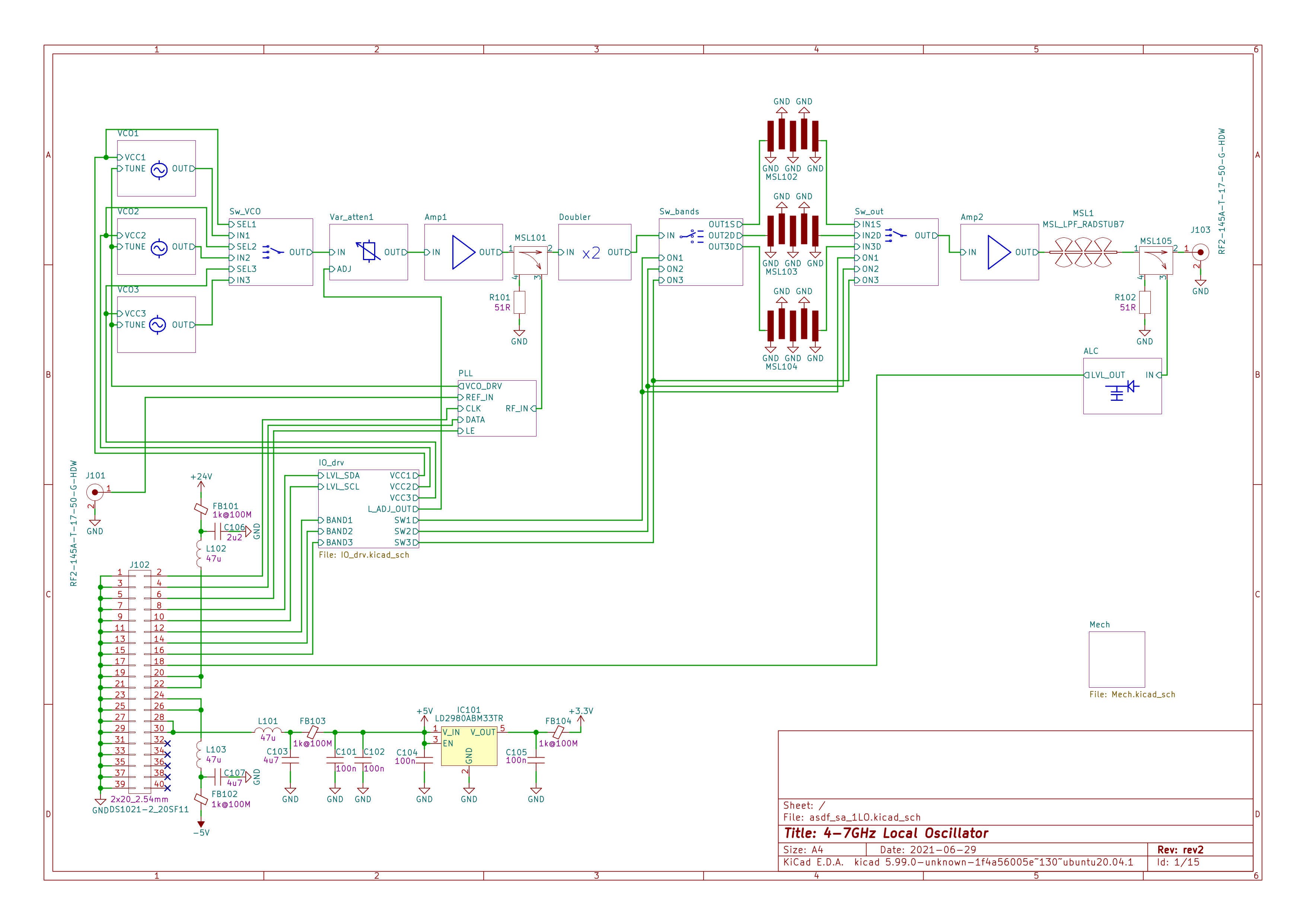
Microwave synthesizer 4-7GHz
Microwave synthesizer - experiments with microwave black magic
 michal777
Become a Hackaday.io member
Already have an account? Log in.
Just one more thing
To make the experience fit your profile, pick a username and tell us what interests you.
Pick an awesome username
hackaday.io/
Your profile's URL: hackaday.io/username. Max 25 alphanumeric characters.
Pick a few interests
Projects that share your interests
People that share your interests
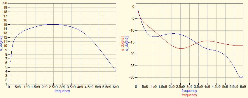
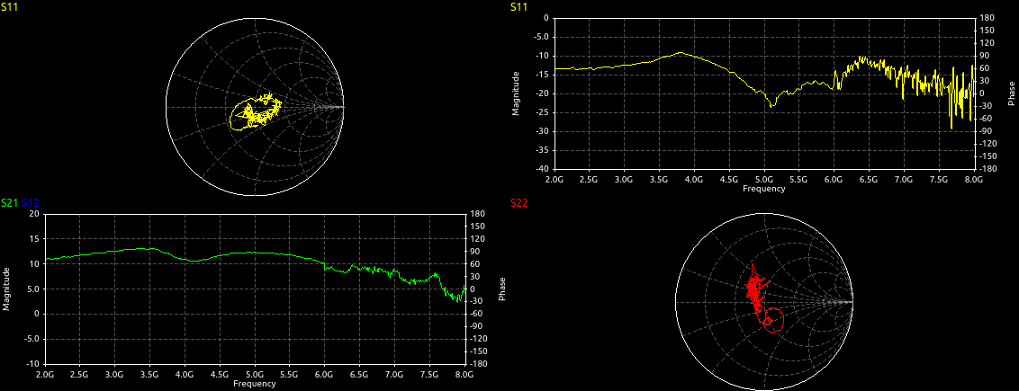
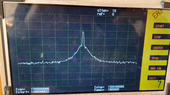
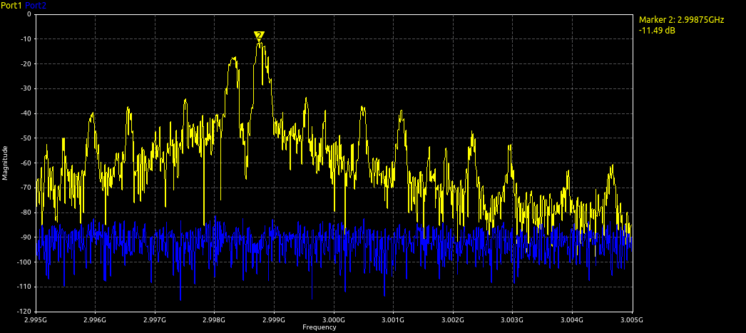 The second test of
VCO is S11 at output. I simply measured VCO using VNA while it
oscillates but I’m not sure if it’s good method. It seems that
the VCO output has low impedance (probably it makes sense – it’s
OC circuit) so adding 50R in series at the output decreases S11.
The second test of
VCO is S11 at output. I simply measured VCO using VNA while it
oscillates but I’m not sure if it’s good method. It seems that
the VCO output has low impedance (probably it makes sense – it’s
OC circuit) so adding 50R in series at the output decreases S11.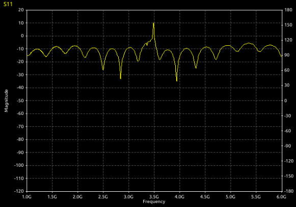
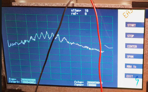
 Full on:
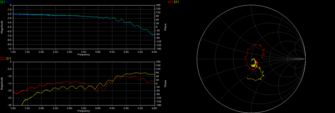
 on
on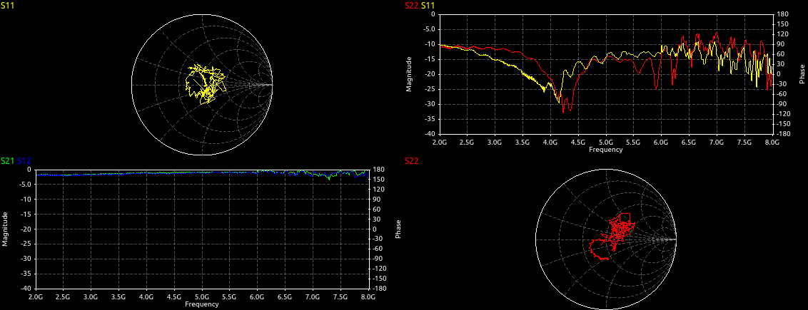 off
off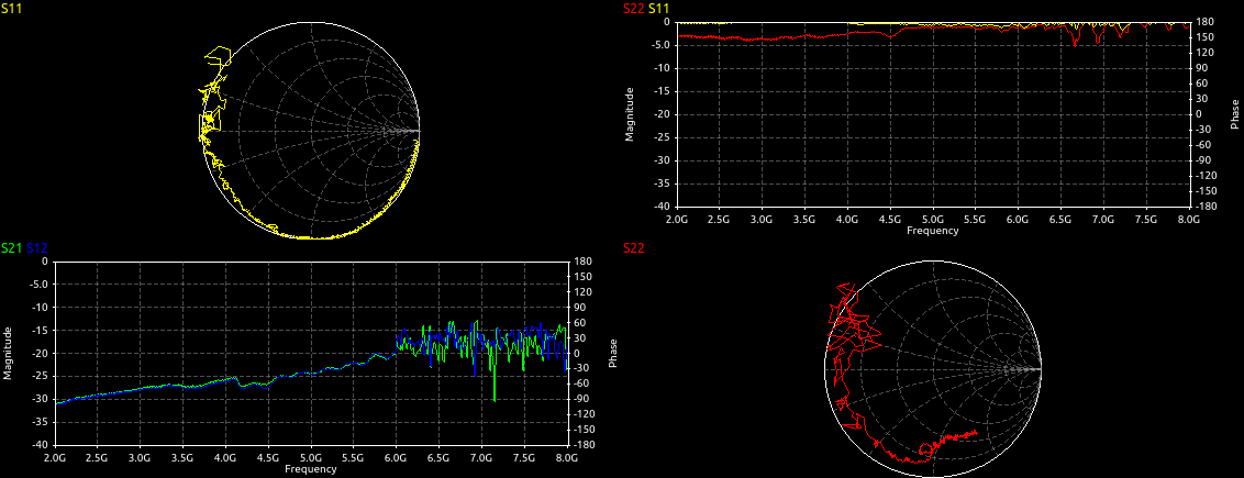


 Richard Dudley
 kevarek
 agp.cooper
 Grant Giesbrecht
Kudos to you for designing the VCO's and amplifiers from discrete transistors!
Why did you decide to use ALC power control in the LO for driving the mixers in the spectrum analyzer? It would be simpler to use 50 ohm gain blocks that are driven a few dB into compression to flatten out power level variations over the LO frequency range. Adding some gain equalizers would also help flatten the power variation. The LO drive to the mixer doesn't require the level of accuracy that an ALC would provide.
I noticed the dual diodes in the ALC level detect circuit. It looks like one diode is used to track the temperature drift of the main one and the differential amp subtracts out the temperature drift. How well does it work?
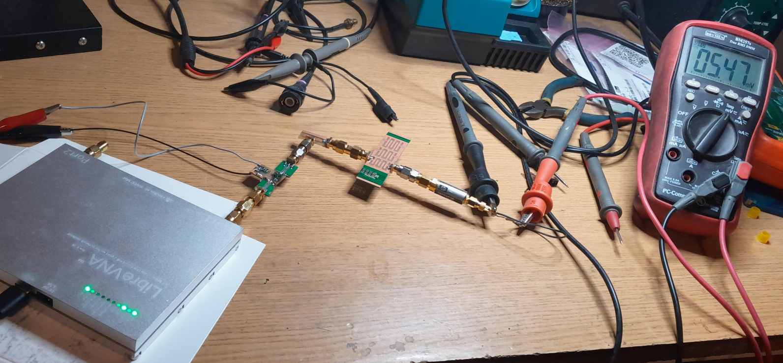
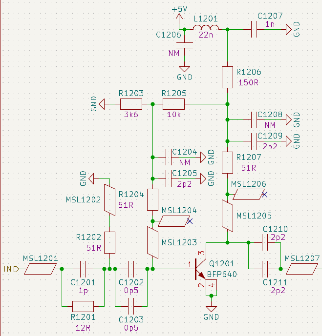
Assuming that your board is going to be covered with a shield, the cavities for the doubler and the circuit before it (a quadrature hybrid?) are very large. Cavity resonances causing spurs would be a concern.