 Tim
TimAs a next step we will look into options to design XOR2 gates in LTL.
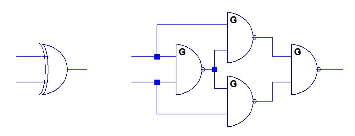 A straightforward approach is to build a XOR2 gate from 4 NAND gates. This is simple and robust, but results in a propagation delay of three NAND2 equivalent. Not perfect for fast circuits. Also, the component consumption is quite high.
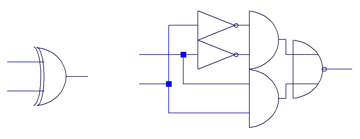
Another option is to use an AOI2 gate and two inverters. The number of components is almost the same as the NAND2 implementation, but now the propagation delay is only two gates. Furthermore, often inverted signals are alrady available as output from a previous stage. In that case, the inverters can be omitted.
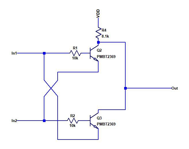 One approach that has been discussed at length at the hackaday TTLers is to use a cross coupled transitor pair, as shown above in a XNOR2 gate. This method is really tricky and drastically reduces the part count. In context of LTL there are a few challenges, though: The gate above is basically an RTL gate and will sink current when the input is high, which leads to a reduced fan-out. The threshold voltage is not defined relatively to ground, but in reference to the second input. The gate switches when the voltage difference between both inputs is equal to Vbe (~0.7V) - very different from the normal LTL threshold. Also, the output low level is 2xVCEsat instead of 1xVCEsat. The combination of all these effects leads to some headaches when designing circuits with several of these XNOR2 gates as they will start to influence each other and the noise margin degrades. A few changes have to be introduced to make this type of gate a bit more compatible to LTL.
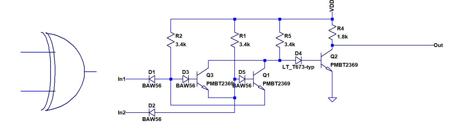
An LTL version of a XOR2 gate based on a cross coupled transistor pair is shown above. First, this device has an output inverter to restore the low level. An input diode and resistor is added to avoid current sinking during high. To fix the threshold levels, two additional diodes were added (D1, D3). LEDs cannot be used in this place, because there are other elements in the current path (D1,D2, output transistor from preceding gate) that add to threshold voltage. The threshold level is still defined by the differential voltage between two inputs. This is still of concern, but a little less relevant now since the output levels have been restored. Assuming the input low level is 1xVCEsat, the threshold level is equal to VD1-VD3+VBE+D2+VCESat: 0.7+0.7+0.2 ~ 1.6V. This is much higher than the 0.7V of the bare transistor, however still not the same as the LTL threshold levels.
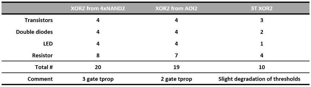 The three options are summarized above. Using a 3T XOR2 gate allows to reduce compenent count drastically, but still comes with some potential to screw up signal integrity. In practice often both inverted and noninverted input signals are available. In that case using an AOI2 gate is the most straightforward option and only adds 9 components.
Discussions
Become a Hackaday.io Member
Create an account to leave a comment. Already have an account? Log In.
I'll have to update the "XOR zoo" with your improved schematic :-)
Are you sure? yes | no