 Tim
TimThere are some ways to simplify the ISA or the datapath, for example by replacing the ADD instruction with something else (think Brainfuck) or reducing datapath width. All of these lead to an explosion in number of instructions needed to perform even the simplest operation, which will in turn increase memory size requirements and hence address path width. A nice example of this extreme are designs like the Qibec, which is a very nicely done implementation of an "invert bit and branch" one bit OISC. While it reduces the datapath to one bit, the address path needs to be increased to 16 bit to allow any meaningful program.
I may rant more about this at a later time, but in essence there seems to be little overall gain for these trade offs and all of them come at a great disadvantage in usability of the instruction set architecture.
I noticed way too late that I was actually not the first to implement the MCPU as a discrete CPU: The ED-64 is a very great looking implementation based on core memory. Kudos to Andrew for this great effort!
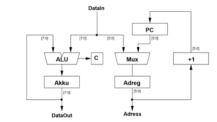
The original MCPU architecture is shown above. There are separate flows for the address and data-path. The state machine is not shown. Since this design is catered for a CPLD, it assumes edge triggered flip-flops for all registers.
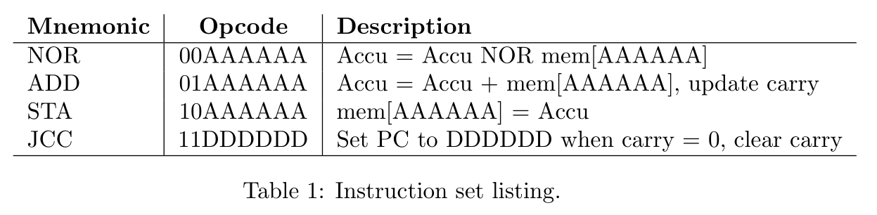
The MCPU programmers model is based on two registers: Accumulator and PC. The ISA consists of four instructions in a fixed encoding that is based on a two bit opcode and a six bit memory address. This ISA can be directly mapped to the datapath shown above with minimal control overhead. See MCPU link for more information including assembler, emulator and example code.
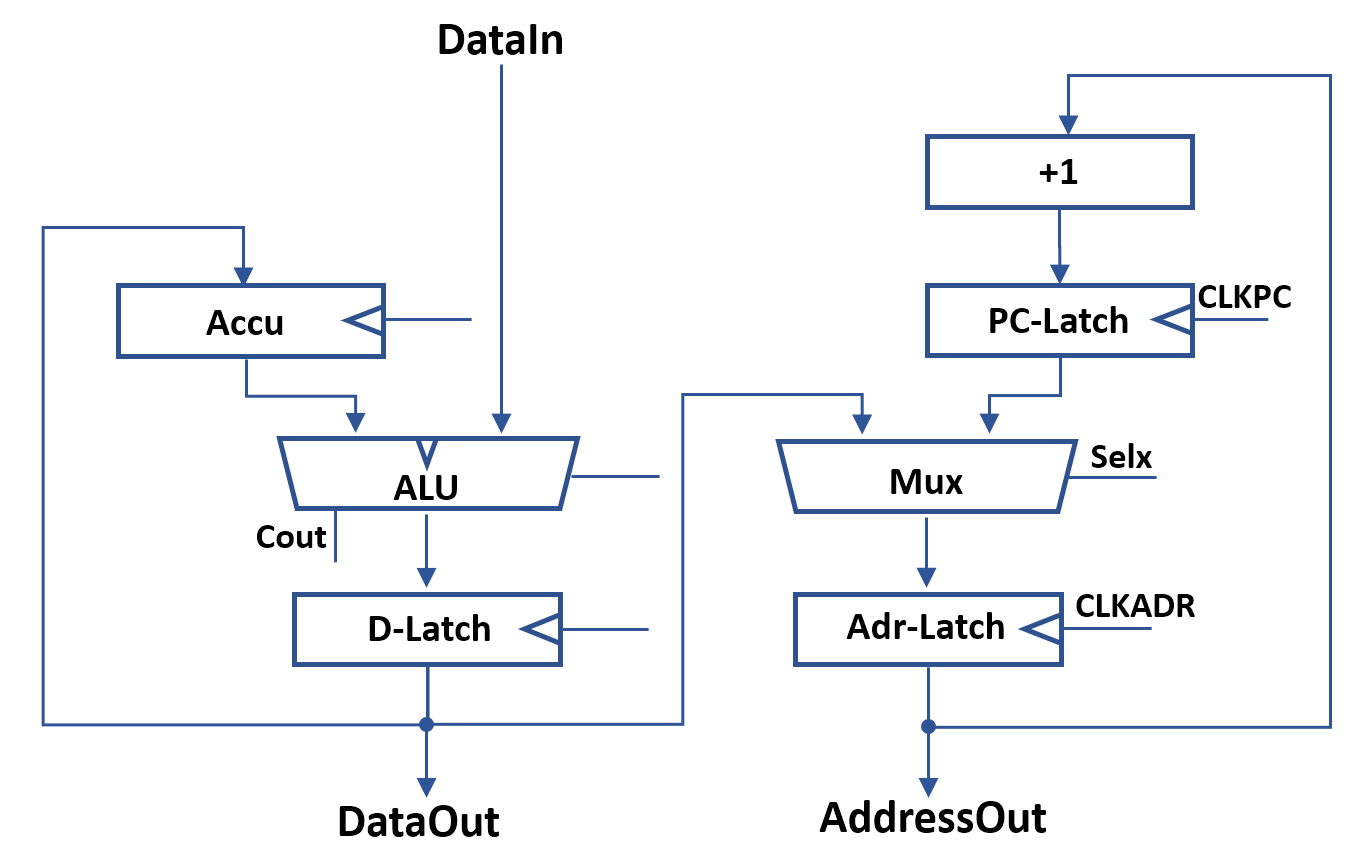
In LTL it is much simpler to use latches instead of edge triggered flip flops. Introducing latches requires changing the design in some places to avoid race conditions where the input of the latch is dependent on its output. This is, for example, the case for the accumulator. The diagram above shows a latch-based architecture. The main modification is the addition of a data latch. The data latch is used to prevent race conditions for memory loads and accu-accu operations.
For implementation, I divided the design into three sections: The address path, the datapath and control. This modular architecture allows some freedom to modifify the CPU at a later time and add more instructions. Both data paths will be implemented in a bitslice architecture. This allows reconfiguring the CPU from 8 (data)/6 (address) to other configurations like 16/12 by just adding more slices.
Discussions
Become a Hackaday.io Member
Create an account to leave a comment. Already have an account? Log In.