 Tim
TimThe assembled control unit already arrived a while ago, but I only got around testing it today.
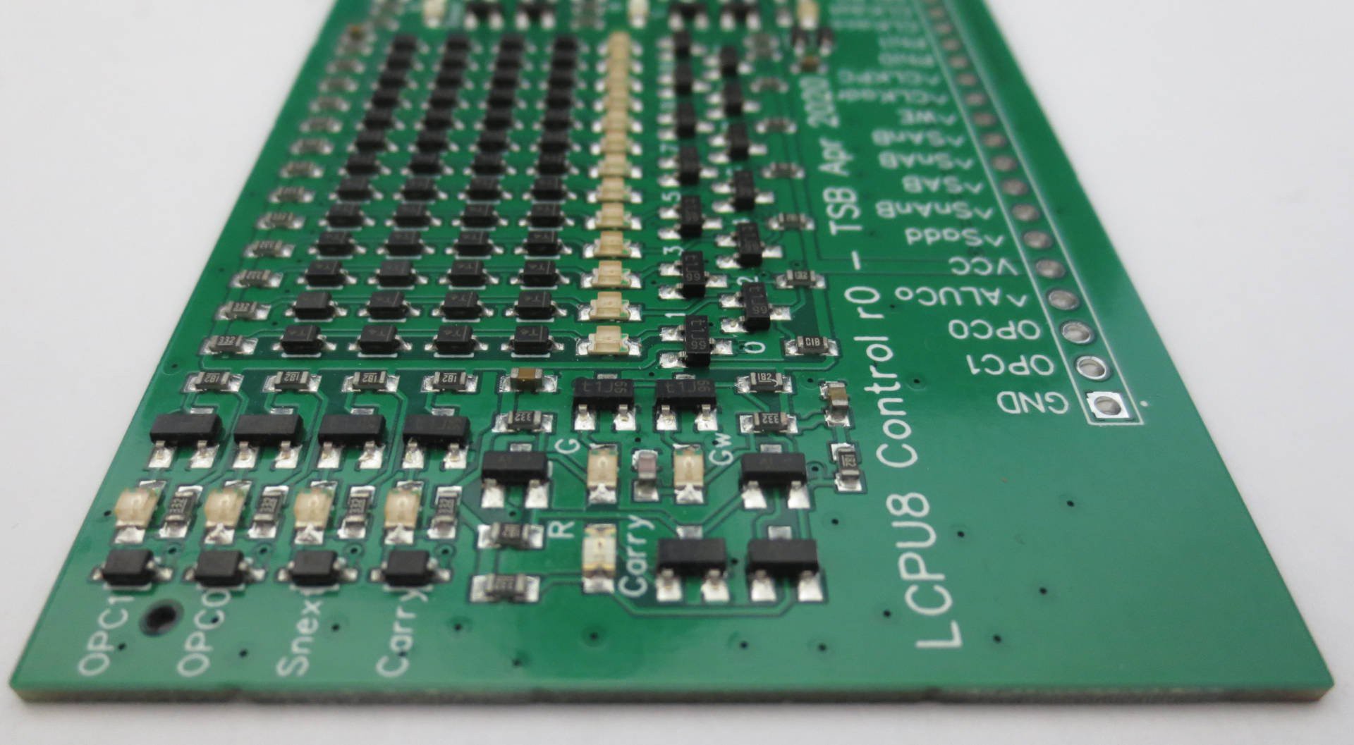
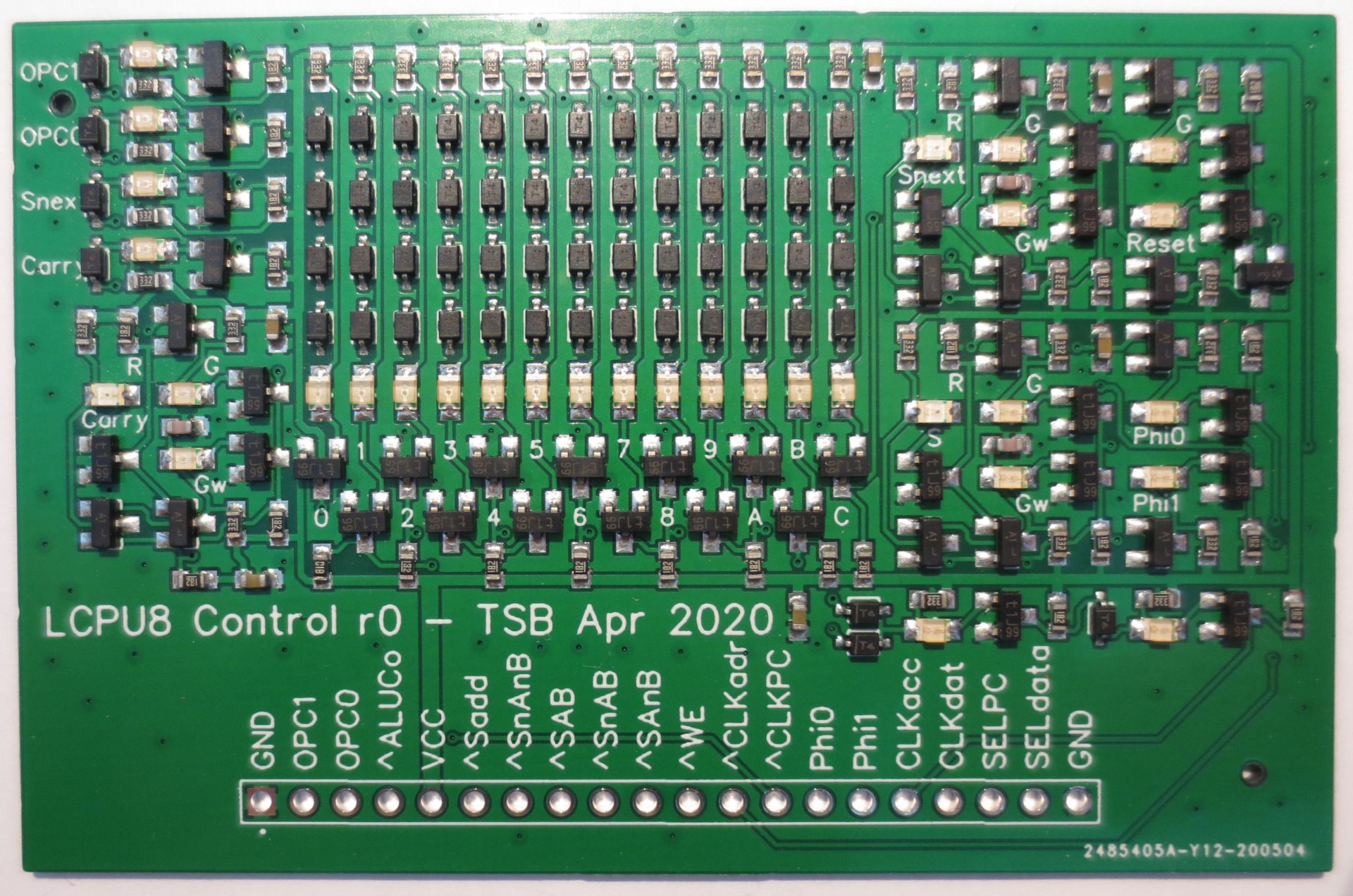 You can see a photograph of the PCB above. Unfortunately I already noticed a stupid mistake at this level: I forgot to route the reset signal to the I/O header. Since this was a circuit level mistake, no DRC caught this. Well, luckily that's easily fixed with an additional wire directly to the reset-driver.
 Due to the construction of the logic array, there is a LED for every row (input) and column (minterm/output), creating a very nice regular structure. Every mintern has an output inverter and uses wired-AND as a combiner. See previous log on control unit design.
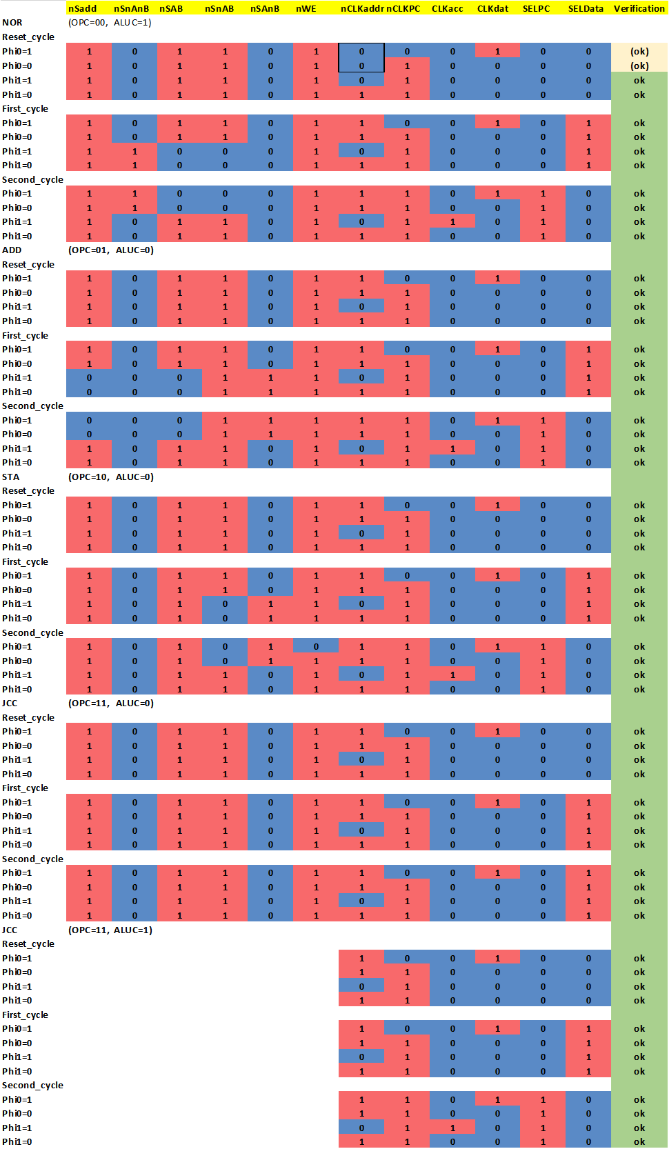
Verifying the control unit is not that easy due to the high number of outputs with irregular behavior in combination with several internal states. I used an ATMega168 microcontroller to exercise every possible sequence and record the outputs.
Each of the four instructions is tested individually, once for carry high and once for carry low. The state of the carry flag only plays a role for the branch instruction. Each instruction test sequence consists of three cycles: In the first cycle reset is high to reset the state registers, then the instruction is clocked for two cycles to exercise both possible instruction states. (I also tested longer sequences to make sure the state machine jumps back to S0)
The full sequences are listed below. The output was verified in the true-and-tested "visual inspection of output waveforms" method, that is still completely ok for designs of this size.
There is a slight misbehvaior of nCLKaddr during the first test sequence, but this is inconsequential and seems to be related to an issue with the test setup. Apart from that, everything was tested to work fine.
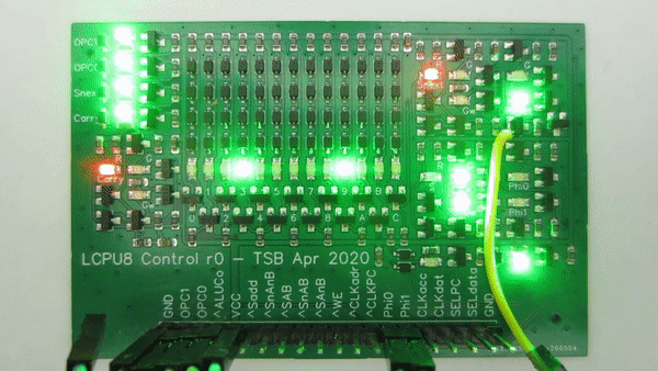 You can see the control unit in action above. Due to it's irregular pattern, this truely seems to be "peak blinkenlight".
The test of the control unit concludes the design of all major functional units of the LCPU: ALU, Adress path and control unit.
Now on to a slightly more annoying part: Designing the backplane board. I still have no idea how to do it in a way that does not obscure all the nice LEDs. Apart from that, the backplane needs to hold the memory and I need to find a way to integrate bootloading and output in an efficient manner.
Discussions
Become a Hackaday.io Member
Create an account to leave a comment. Already have an account? Log In.
I love it! Those look like some bright LEDs though. I would have gone with ones that weren't so bright.
Are you sure? yes | no
Thanks! The high brighness is to some extend only relative, due to low ambient illumination. The LEDs are actually only driven at 1 mA or so, and that is also needed to get fast switching. There are not many options to select less efficient LEDs...
Are you sure? yes | no