 Lincoln R.
Last week I saw a post on Reddit where somebody successfully ported a CP/M clone they wrote to run on of all things a typewriter. This caused me to remember that the same manufacturer produced a line of laptop form factor word processors. A 1990s word processor with all its software built into mask ROM wouldn't normally be too exciting, but the specifications of this piece of hardware could actually make for a pretty nice CP/M portable:
- Bitmapped LCD display at 640 x 200 resolution
- Serial and parallel ports built in
- 1.44 MB floppy drive
- Internal battery
- Some quantity (at least 32KB) of RAM
- A lot lighter than a Kaypro or Osborne


 Jac Goudsmit
 Keith
Keith
 Howard Jones
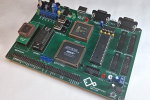
 Colin Maykish
Hi Jim,
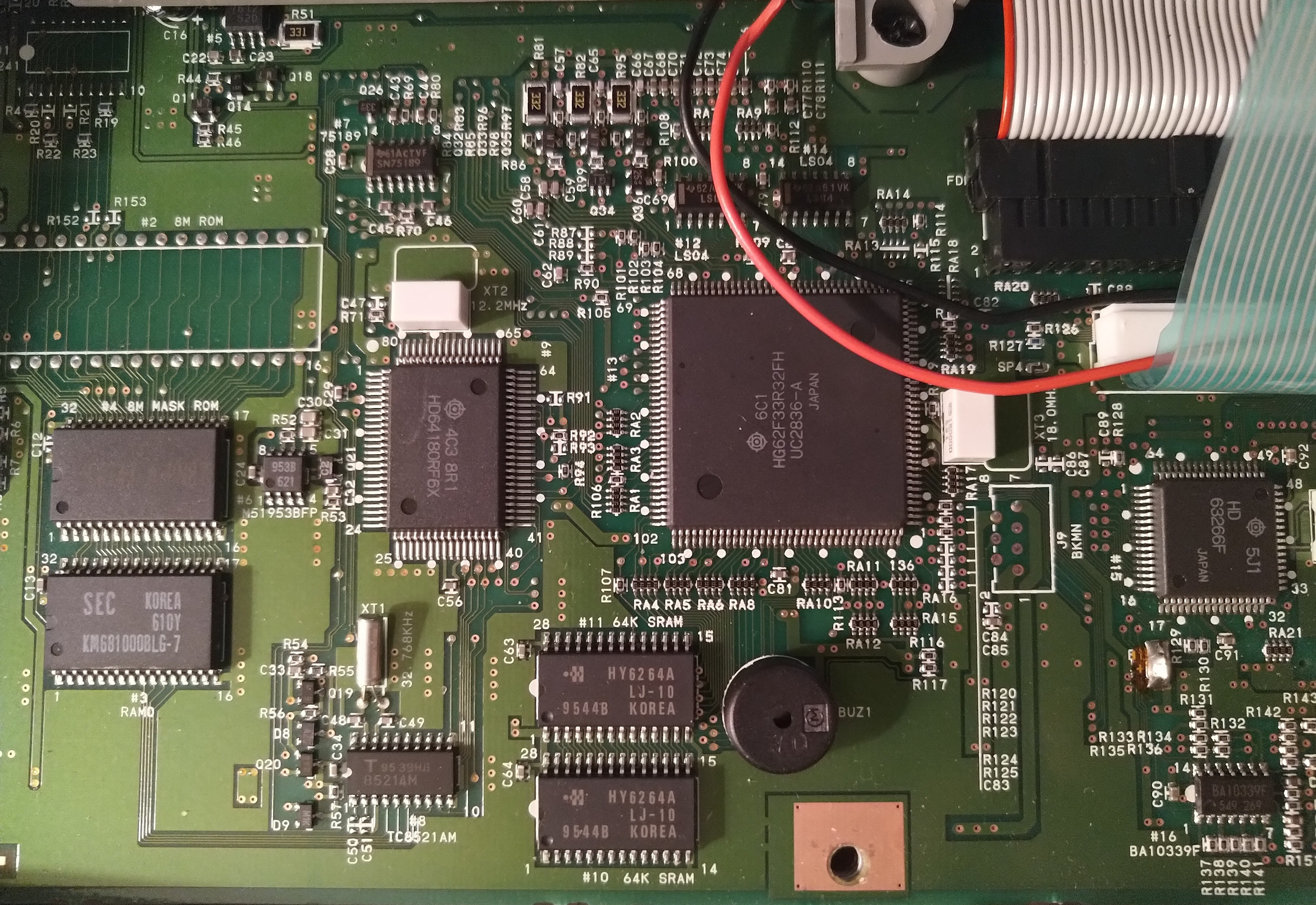
Sorry I didn't respond to your earlier comment. I had started on this project then other aspects of my life got really busy and I haven't had time to revisit it. Thanks for pointing me to your ROM dump. I suspect the 8800 and 8700 hardware are actually pretty similar, especially given that the custom gate array has the same part number on it (I'm guessing the UC2836-A is the Brother part number for the specific mask programming of that gate array given that they used UC2xxx part numbers on the mask ROMs).
How did you end up dumping your ROM? I suspect the pinouts are almost certainly the same, did you remove the chip and use a chip programmer, or hook up wires to some microcontroller board to dump it? I'm happy to try dumping mine sometime.
I wonder what the upside-down mounted DIP IC on your Bookman daughtercard is. I've never looked that extensively at the Bookman hardware but you can tell that chip was clearly added on as an after-the-fact hack. My guess based on the wiring is that it's some 7400 logic gate IC.