0%
0%
FUSBee5
FPGA module featuring an ECP5, dual Hyperram, USB 3.0 and 48 IOs.
Become a Hackaday.io member
Already have an account? Log in.
Just one more thing
To make the experience fit your profile, pick a username and tell us what interests you.
Pick an awesome username
hackaday.io/
Your profile's URL: hackaday.io/username. Max 25 alphanumeric characters.
Pick a few interests
Projects that share your interests
People that share your interests
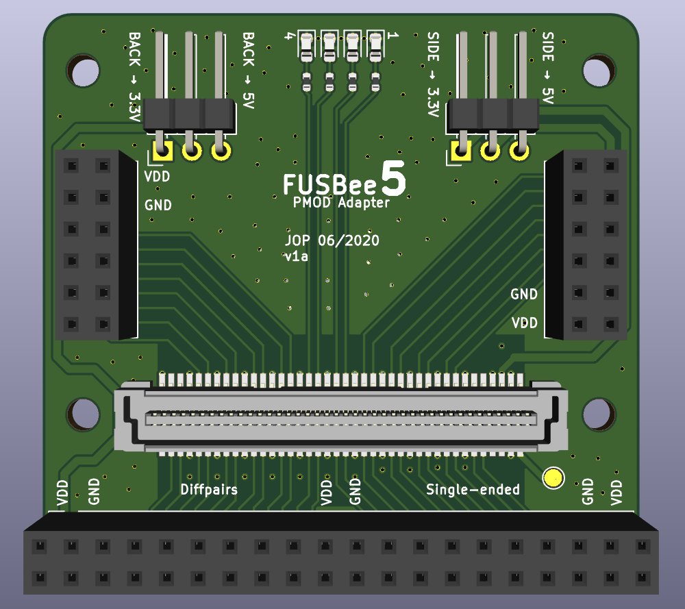 For ease of use and accessibility the headers (especially left and right) should be 90° angled (but the silkscreen for the straight ones is less crowded so I used it here). On the top are 4 additional LEDs for status indications. All signal traces are routed over a solid gnd plane, but without any length matching and impedance consideration (on 2 layers...yeah...).
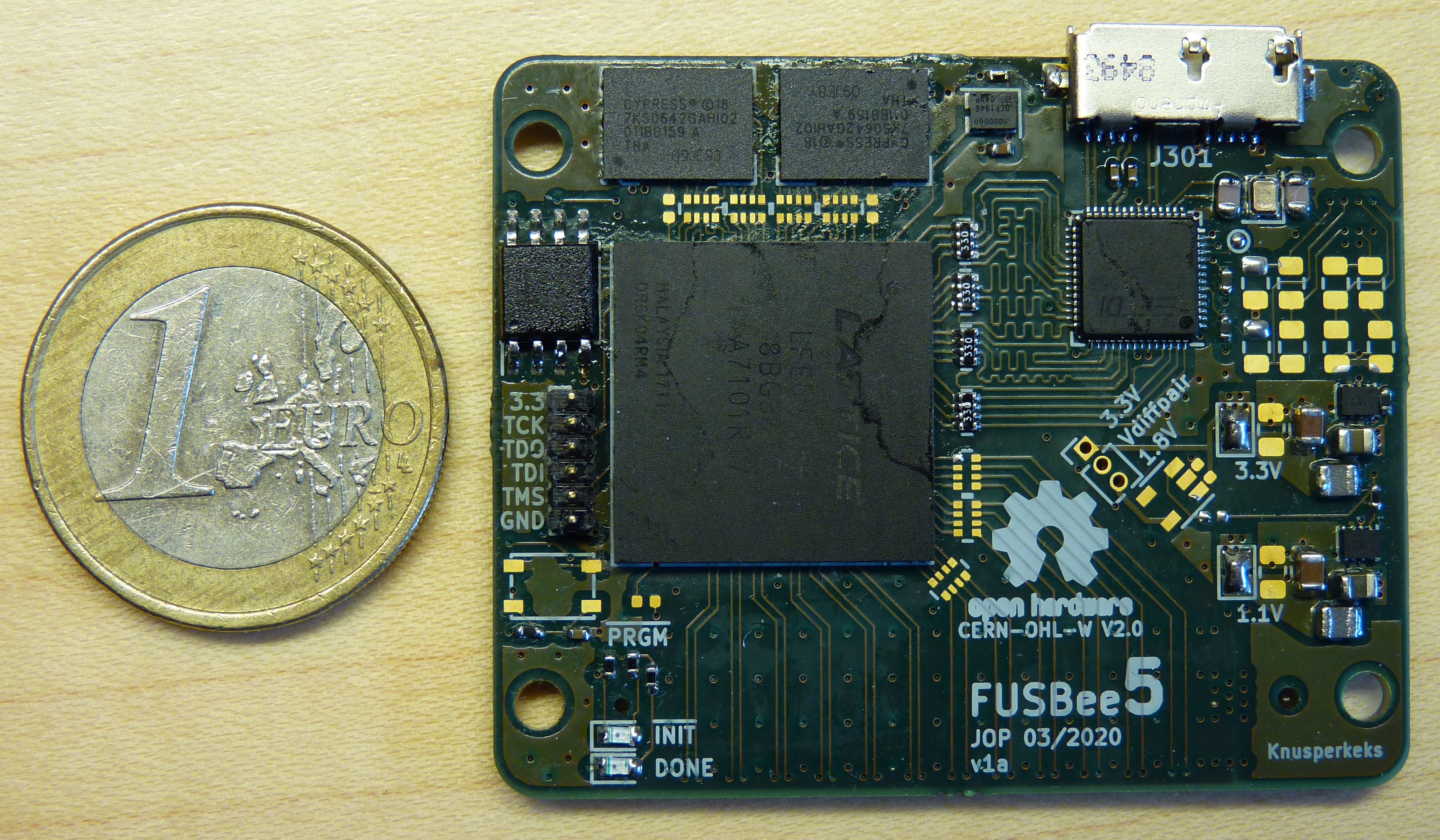
")
 Dave Collins
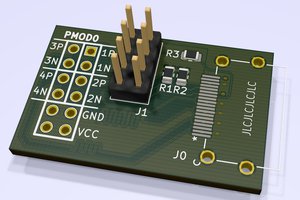
 Maya Posch
 The Big One