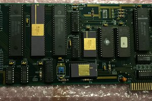
EtchedPixels
The biggest challenge with this board was space. It's still a bit larger than a standard RC2014 card and the only way to get it into size would be to stack the ROM on the RAM or similar ugliness.
To keep the decode down to a minimum the secondary processor does not decode the I/O space. All of it is a single 16bit write port (A15-A8 being the other bits latched), and 8bit input port. The 8 data bits are visible to the host CPU on an I/O port, the other bits set the ROM on/off and control memory banking and an optional interrupt.
The host side is very similar but is decoded and the upper address lines allow the host to control reset, NMI and IRQ on the coprocessor. At boot the latches reset to zero leaving the CPU shut down. The host then sets the lines high and checks for data activity indicating the board is running.
The secondary CPU memory map is 32K ROM low, 32K RAM high. The ROM can be mapped out giving access to 64K of RAM. The upper address bits are taken from a latch writable by the secondary processor, along with the ROM on/off.
The I/O ports are built out of a 74HCT273 and 74HCT574 parts. The 273s (U6,U7) are used because they have a reset pin and they latch the upper bits of the master and secondary address bus in order to manage control signals. A pair of 74HCT574s (U8, U9) one facing each way act as the 8bit data interface between the host and secondary.
On the host side a 74HCT688 (U2) is used to match the address and half a 74HCT32 (U1) is used to generate read/write lines for the latches. On the secondary side the arrangement is the same except that the address is not decoded and any I/O read or write activates the latches.
For the secondary itself a Z80 (U3) is wired up pretty much as standard. The uninteresting signals are pulled high (BUSRQ, WAIT), the reset, nmi and interrupt come from the latches, clk comes from the host and needs to (otherwise we might read and write the port as it's changing). The address and data bus go direct to a 27C256(U5) and 512K SRAM(U4). Decode is done by a 74HCT139 (U10). One half of it generates a ROM chip select by looking for \MREQ, A15 low and ROMEM (from the latches) low. The other half is used as an inverter to generate the RAM CS for any other state.
There are a some changes that I may make. The spare output latches really should go to headers so they can be used as things like a bitbanged debug port. The 27C256 could be replaced with a 28C64 or 28C256 for simpler programming.
 Keith
Keith
 David Robinson
 Plasmode