 Michael Möller
Status
I now unconditionally copy Register A into Result (what 2nd argument points to) to test my write back.
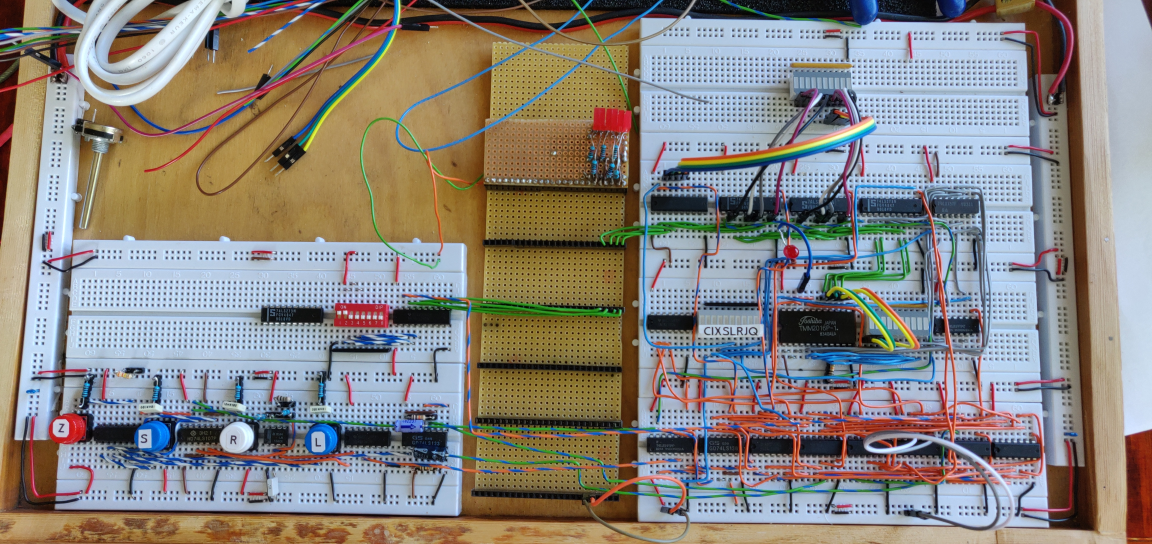
The "bus" in the middle will have LEDs for all 24 lines, when I get to a CPU project with 8 data 16 address. At the moment 4 bit databus.
I have reaaranged a little (as described in previous log) but I am NOT happy with the layout as a whole. Implementation is "organic growth", but I do not want to rearrange everything or every step. The jumperwires are for temporary fixes (like LEQ tied low, as there is no SUB to generate the signal yet, but I can still test how it would work on the µ-sequencer)
Ooops ?
At this point I discover a few (more) errors in the design <sigh>
- µstep5 needs the SXP else it loads random data.
- Total misunderstanding - I have indirection on the jump, too, ie it jumps to the location of the content of what the 3rd arguments point to. Great for subroutines and such like, but very difficult when you do not want a jump, even if the result is negative (which is quite often).
- Using "0" as the special location required a multi input NOR, which required too many chips, so that changes to "-1". (I afterwards noticed this was assumed by some other emulator implementations, too).
- There was no HALT condition in the diagrams, only loosly planned in my head
- The INP is LSB on left, LEDs are LSB on right.
- POTENTIAL - Unsafe conditions like DOD & WRE ( & DATA ) changing simultaneously - ignoring it for the while being
Updated design
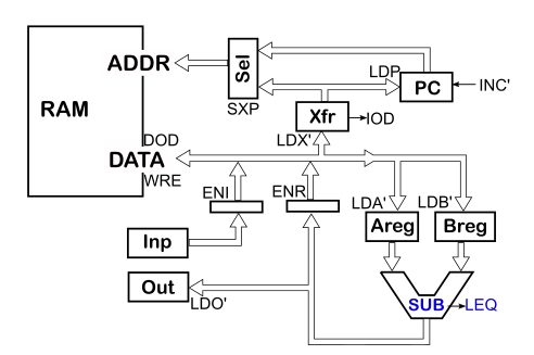
Block schematic
| Units | Signals | ||
|---|---|---|---|
| RAM | Memory | ADDR | Address to memory |
| SEL | Select address source | DATA | bidirectional data (a bus) |
| INP | Input, currently DIP switch | SXP | Select XFR or PC as source for ADDR |
| OUT | Output Buffer (goes to display) | LDP | Load PC with new value |
| XFR | Transfer Buffer, for the indirect arguments | INC' | Increment PC |
| PC | Program counter | IOD | Input/Output-Detect, ie address is -1 |
| Areg | A register | LDX' | Load the XFR register |
| Breg | B register | DOD | DataOutputDeny (=not RAM on Databus) |
| SUB | Subtraction unit | WRE | Write Enable |
| Notes: In these schematic the signals are all positive. (In the circuit half are negative=true) The '-mark is for edge triggered (otherwise they are static levels) | ENI | Enable Input (INP on databus) | |
| ENR | Enable Result (SUB on databus) | ||
| LDA' & LDB' | Load A and B register, respectivly | ||
| LDO | Load Output Register | ||
| LEQ | Less-or-Equal result in SUB | ||
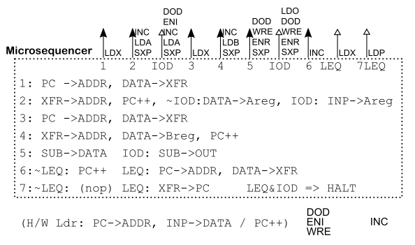
Microsequencer
Signals activation by step above the box, with hollow arrows show the alternative on a condition being true. The listing shows data flow, and the last is the special event when pressing the "load"-button (two pulses generated, not the clock)
Microsequencer-clock-"decoder"
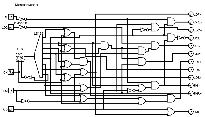
This shows the complex truth with negative/positive and static/edge logic mix. The output suffixes mean "~"inverted, "+"ve and "-"ve edge. The LD1 and LD2 are the two pulses from the manual Load button. The counter reset takes away the 8th redundant µstep, and I should do it for the nonbranch 7th step, too, but I've run out of room for more gates.
Next Planned Step(s)
in the probable order
- Implement the corrections
- The IOD circuit (one multi-input AND)
- The ALU (adder plus inverters)
- LEQ circuit
- OUT connection plus some display
And when it runs, extend to 8 bit data/addr and loading of programs from Arduino
Discussions
Become a Hackaday.io Member
Create an account to leave a comment. Already have an account? Log In.