Close
0%
0%

Microcoding for FPGAs

A microcode compiler developed to fit into FPGA toolchain and validated to develop CDP1805-like CPU and text-based video controller

Similar projects worth following
Make creation of complex CPUs and other controllers easier by extending the usual FPGA toolchain with a new tool: microcode compiler.

Microcode compiler converts a symbolic, macro-assembler like language (common for ANY CPU or controller!) into 2 memory blocks of any size:

- "mapper" that maps higher level CPU instructions into start points of microcode routines
- "microcode" that describes steps in executing a higher level instruction

These two are consumed by a standardized, auto-generated control unit (see digisim illustration) which can be dropped into the design, along with the 2 memory maps above. These 3 components can make up over 50% of any design, the remaining is specific / custom, but even that follows simple rules.

To validate, a CDP1802 microprocessor and TTY to VGA controller have been written and are free to use (see gallery for samples of BASIC code test runs)

I will try to document to some level of detail in project blogs here.

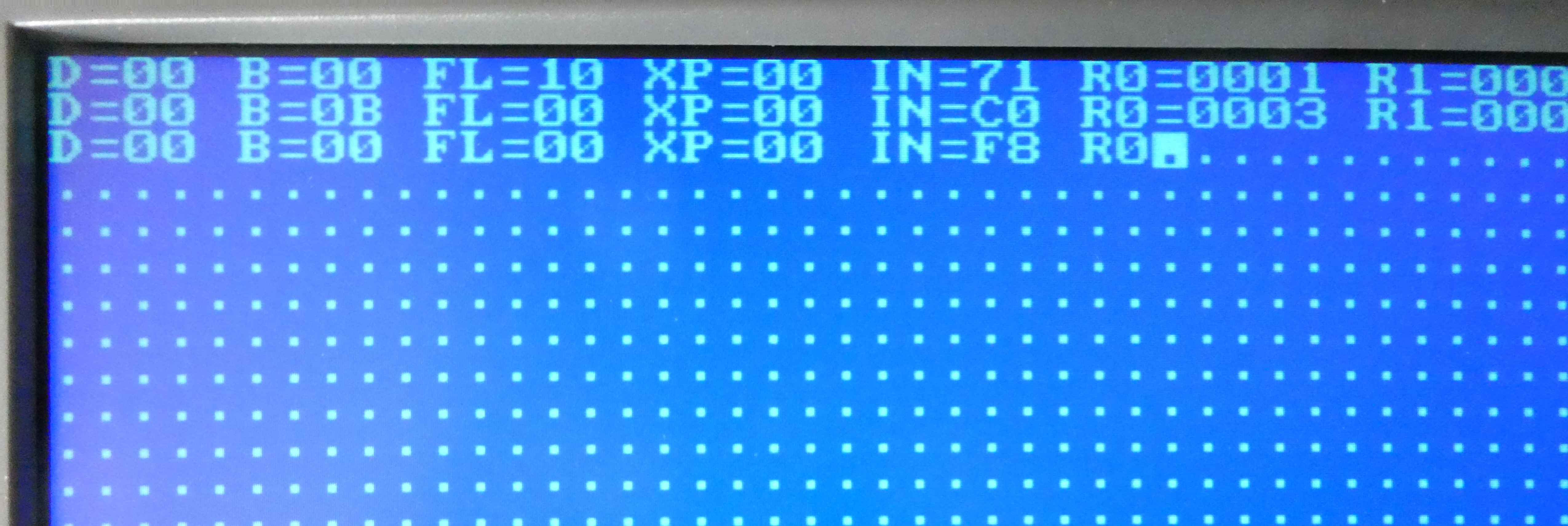
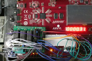
Demo session, uploading the bit file (which is inside the sys_180x*.zip) to Digilent Anvyl board, and running Monitor and Basic. Both the CPU and the TTY to VGA controller have been programmed using the microcode compiler.  

Sys_180X (7).zip

Pretty raw archive of the ISE14.7 project creating a small system with CDP180X implementation - it runs Monitor (http://www.sunrise-ev.com/MembershipCard/MCSMP20.pdf) and BASIC (http://www.sunrise-ev.com/MembershipCard/BASIC3v11user.pdf) . Check the attached screenshots.

x-zip-compressed - 27.88 MB - 07/02/2020 at 05:37

Download

sys180x_anvyl.bit

Bitstream for Anvyl board (use Digilent Adept to upload to the board)

bit - 1.42 MB - 07/02/2020 at 05:29

Download

benchmark8.bas

Simple test program in Basic

bas - 531.00 bytes - 07/02/2020 at 05:28

Download

mcc_control_unit.circ

Logisim schema of the control unit. To download logisim: http://www.cburch.com/logisim/

circ - 18.75 kB - 06/07/2020 at 18:12

Download

  • 1 × https://store.digilentinc.com/anvyl-spartan-6-fpga-trainer-board/ Used to develop and tun proof of concept designs
  • 1 × https://visualstudio.microsoft.com/ Used to develop compiler in C#
  • 1 × https://www.xilinx.com/support/download/index.html/content/xilinx/en/downloadNav/vivado-design-tools/archive-ise.html FPGA development suite
  • 1 × https://store.digilentinc.com/digilent-adept-2-download-only/ To program the board with .bit file

  • More controllers implemented in microcode!

    zpekic09/16/2021 at 04:03 0 comments

    What is the difference between a "controller", and "dedicated CPU"? Essentially nothing - from the perspective of microcoded design they can be developed, debugged and operated in the same way. Here are two additional controllers from my other project:

    1. HEX2MEM - processes ASCII character stream in real time (interpreted as Intel HEX file), to write to RAM 
    2. MEM2HEX - read up to 64k of RAM/ROM, and generate ASCII stream (in Intel HEX format).

    Note that both of these are written with an updated, less buggy version of microcode compiler

  • Boilerplate VHDL code generation from microcode

    zpekic11/15/2020 at 07:28 0 comments

    As I started working on a new design, I realized quite a bit of VHDL code needed could be generated by the microcode compiler itself. 

    Typically, a micro-coded CPU/controller contains:

    1. control unit (generated using .controller statement)
    2. microcode store (generated using .code statement)
    3. instruction mapper store (optional, generated using .mapper statement)
    4. various registers that need to be updated from different sources (register + MUX)
    5. internal components (such as ALUs) fed from different sources (MUX)
    6. various lookup tables / ROMs
    7. other combinatorial logic

    The guiding principle behind my microcode compiler and associated hardware is  a pattern and template oriented approach as a trade off between increased productivity and quality vs. somewhat less flexibility and compactness. To keep with that design philosophy I improved the compiler so that in addition to 1. - 3. above it can also generate boilerplate for .4. and 5.

    Basic idea is to generate a (commented) boilerplate VHDL code which developer can choose to copy and paste into the design and modify there as needed.

    While there is an extra copy/paste step, the beauty of this approach that no tooling updates or touches the human developed code, they remain independent. 

    Below are some examples:

     run "mcc CDP180X.mcc" to generate:

    cdp180x_code.vhd

    cdp180x_map.vhd

    cpu_control_unit.vhd


    Condition codes

    The control unit requires a single bit to determine if the then or else instruction will be executed. This is described in the microcode using .if instruction:

    seq_cond:		.if 4 values 
    				true, 			// hard-code to 1
    				mode_1805, 		// external signal enabling 1805/1806 instructions
    				sync,			// to sync with regular machine cycle when exiting tracing routine
    				cond_3X,		// driven by 8 input mux connected to ir(2 downto 0), and ir(3) is xor
    				cond_4,			// not used
    				cond_5,			// not used
    				continue,		// not (DMA_IN or DMA_OUT or INT)
    				continue_sw,	// same as above, but also signal to use switch mux in else clause
    				cond_8,			// not used
    				externalInt,	// for BXI (force false in 1802 mode)
    				counterInt,		// for BCI (force false in 1802 mode)
    				alu16_zero,		// 16-bit ALU output (used in DBNZ only)
    				cond_CX,		// driven by 8 input mux connected to ir(2 downto 0), and ir(3) is xor
    				traceEnabled,	// high to trace each instruction
    				traceReady,		// high if tracer has processed the trace character
    				false			// hard-code to 0
    				default true;

    This results in VHDL code that can be copied into control unit instantiation and hooked up to the various test points in the design (note how "true" and "false" have been recognized and turned into '1' and '0'):

    ---- Start boilerplate code (use with utmost caution!)
    ---- include '.controller <filename.vhd>, <stackdepth>;' in .mcc file to generate pre-canned microcode control unit and feed 'conditions' with:
    --  cond(seq_cond_true) => '1',
    --  cond(seq_cond_mode_1805) => mode_1805,
    --  cond(seq_cond_sync) => sync,
    --  cond(seq_cond_cond_3X) => cond_3X,
    --  cond(seq_cond_cond_4) => cond_4,
    --  cond(seq_cond_cond_5) => cond_5,
    --  cond(seq_cond_continue) => continue,
    --  cond(seq_cond_continue_sw) => continue_sw,
    --  cond(seq_cond_cond_8) => cond_8,
    --  cond(seq_cond_externalInt) => externalInt,
    --  cond(seq_cond_counterInt) => counterInt,
    --  cond(seq_cond_alu16_zero) => alu16_zero,
    --  cond(seq_cond_cond_CX) => cond_CX,
    --  cond(seq_cond_traceEnabled) => traceEnabled,
    --  cond(seq_cond_traceReady) => traceReady,
    --  cond(seq_cond_false) => '0',
    ---- End boilerplate code

    MUX, 2 to 1

    alu_cin:	.valfield 1 values f1_or_f0, df default f1_or_f0;	// f1_or_f1 will generate 0 for add, and 1 for subtract

    becomes (note the pattern to check when clause for non-default):

    ---- Start boilerplate code (use with utmost caution!)
    --	alu_cin <= df when (cpu_alu_cin = alu_cin_df) else f1_or_f0;
    ---- End boilerplate code

    MUX, 2^n to 1

    sel_reg:	.valfield 3	values zero, one, two, x, n, p default zero;		// select source of R0-R15 address

    becomes (note...

    Read more »

  • Microcode Compiler quick manual

    zpekic07/05/2020 at 04:58 0 comments

    Disclaimer: The work on the MCC is still ongoing / evolving, so the current state on github may deviate from the description below. 

    There is no install package for mcc.exe - it is a simple command line utility which will work on most versions of Windows, and can probably be also recompiled for other platforms that have .net and C# ported.

    INVOKING THE COMPILER

    Starting with -h command line argument lists the usage:

    >mcc.exe -h
    --------------------------------------------------------
    -- mcc V0.9.0627 - Custom microcode compiler (c)2020-...
    --    https://github.com/zpekic/MicroCodeCompiler
    --------------------------------------------------------
    
    Compile mode (generate microcode, mapper and control unit files):
    mcc.exe [relpath|fullpath\]sourcefile.mcc
    
    Convert mode (generate sourcefile.coe, .cgf, .mif, .hex, .vhd files):
    mcc.exe [relpath|fullpath\]sourcefile.bin [addresswidth [[wordwidth [recordwidth]]]
    addresswidth   ... 2^addresswidth is memory depth (integer, range: 0 to 16, default: 0 which will infer from file size)
    wordwidth      ... memory width (integer, values: 8, 16, 32 bits, default: 8 (1 byte))
    recordwidth    ... used for .hex files (integer, values: 1, 2, 4, 8, 16, 32 bytes, default: 16)
    
    For more info see https://hackaday.io/project/172073-microcoding-for-fpgas

    The convert mode allows usage as a handy utility to convert memory file formats that often come up in FPGA or other embedded system development. The focus here will be on the usage to generate elements of the microcoded design ("compile mode").


    GENERAL SYNTAX RULES FOR SOURCE.MCC

    The mcc source file is a text file with extension .mcc with few general rules:

    • each statement must end with ;
    • statements can go into multiple lines (encouraged for clarity)
    • if the statement is a microinstruction, a comma delimits a microcode field, and semicolon the instructions, meaning "1 semicolon = 1 microcode cycle"
    • labels end with colon (by convention, but not enforced), and follow the usual rules (can start with _ or alpha characters, but may contain no special characters except _)
    • labels starting with _ cannot be jumped to (this is useful to explicitly forbid some jump destinations)
    • everything is case-insensitive (but lowecase is encouraged)
    • comments - everything after // until end of line is ignored. Currently, no multi-line comments are supported
    • constants can be given as decimal, hex (0x...), octal (0o...), or binary (0b...). In some cases (for example .org), the binary/octal/hex can contain ? wildcard, which indicated 1, 3, or 4 "don't care" bits. In addition 'char' constant will be represented by its basic ASCII code.
    • from the compiler perspective, source.mcc contains only:
      • statements (keywords starting with dot)
      • microinstructions


    STATEMENTS

    Following statements are currently recognized by mcc.exe:

    Design definition statements:

    .code depth, width, filelist, bytewidth;

    Reserves memory for microcode:

    • 2^depth will be the number of words
    • each word will be <width> words wide - this must be equal or bigger than the sum of all the field widths
    • successful compile will produce all the files in the <filelist>, they will all contain same data but described according to file format
    • <bytewidth> will be used for .hex file format to have that record size (must be equal or greater than <width>

    Example: generate 5 files describing the 64 * 32 memory containing the generated microcode:

    .code 6, 32, tty_screen_code.mif, tty_screen_code.cgf, tty:tty_screen_code.vhd, tty_screen_code.hex, tty_screen_code.bin, 4;

    .mapper depth, width, filelist, bytewidth;

    Reserves memory for mapper - this is the lookup memory that accepts bit patter from instruction register as address, and outputs the starting address of microcode implementing that instruction. The arguments are same like for .code statement

    Example: generate 5 files describing the 128 * 6 memory containing the generated mapper:

    .mapper 7, 6, tty_screen_map.mif, tty_screen_map.cgf, tty:tty_screen_map.vhd...
    Read more »

  • Microcode compiler in FPGA toolchain

    zpekic06/14/2020 at 00:56 0 comments

    TL;DR

    In case you want to skip much theory below and dig-in in a practical way, follow this guide: https://hackaday.io/project/182959-custom-circuit-testing-using-intel-hex-files/log/201614-micro-coded-controller-deep-dive


    The following diagram above illustrates the high-level code / project flow that uses mcc microcode compiler. Details are elaborated below.

    source.mcc

    Microcode source code file is a simple text file that typically contains following sections:

    • code memory description (.code statement)
    • mapper memory description (.mapper statement)
    • microinstruction word description containing:
    • sequencer description (.if .then .else)
    • values available in current microinstruction clock ( .valfield)
    • values available in next microinstruction clock (captured at next clock: .regfield)
    • simple macros (.alias)
    • microcode statements. These are:
      • put into specific microcode locations using .org statement
      • mapped to specific instruction patterns using .map statement
      • containing any number of value and/or register assignment, but only up to 1 if-then-else statement
      • commas can be read as "simultaneous in 1 clock cycle", and 1 semicolon maps to 1 cycle

    A single statement can go into any number of lines for clarity, but last one must be terminated by a ;

    Labels can stand in front of aliases to be used ("expanded") in code later, or in front of microcode statements, to be used as target to goto/gosub (except _ starting labels to prevent that on purpose, for example first 4 cycles after reset)

    mcc.exe

    This is a 2-pass, in-memory compiler written in pretty straightforward C# / .Net that should make it portable to other platforms (although this has not been evaluated)

    There are 2 modes to use it:

    1. compile (mcc.exe source.mcc) to generate code/mapper memory files
    2. convert (mcc.exe source.bin [addresswidth] [wordwidth] [recordwidth])

    Both will produce extensive warning and error list on the console, as well as source.log file with detailed execution log.

    Currently, only conversion from bin (for example, EPROM image) is supported, but I plan to add other file formats too. Conversion parameters are:

    • addresswidth - integer (default = 0 (auto-size)) - number of locations in the memory block
    • wordwidth - integer (default = 8) - number of bits in one word
    • recordwidth - integer (default = 16) - number of bytes per line in .hex file output


    Generated files

    In order to facilitate ease of use in standard vendor or open-source FGPA toolchain downstream, multiple data format files are generated. All contain same information though!

    The .code, .mapper, .controller statements describe the files generated:

    .code 6, 32, tty_screen_code.mif, tty_screen_code.cgf, tty:tty_screen_code.vhd, tty_screen_code.hex, 4;
    .mapper 7, 6, tty_screen_map.mif, tty_screen_map.cgf, tty:tty_screen_map.vhd, tty_screen_map.hex, 1;
    .controller cpu_control_unit.vhd, 8;

    This will generate:

    A code memory block of 64 words 32 bits wide, and store it to following files:

    • tty_screen_code.mif - useful for Altera/Intel tools
    • tty_screen_code.cgf - for Xilinx
    • tty_screen_code.coe - for Xilinx (not specified in the statements above so not generated, link is to equivalent file from CDP180X.mcc)
    • tty_screen_code.vhd - a "VHDL Package" good for all FPGA compilers, can be included in the list of project files (the "tty" prefix allows any number of microcoded design to be included into same FPGA project, differentiated by this prefix)
    • tty_screen_code.hex - useful for any tools, including possibly loading into the FPGA ("dynamic microcode!") during runtime. The paramer "4" indicates 4 bytes per line (usually is 16 for .hex files)

    A mapper memory block 128 words, 6 bits wide, files similar to above.

    The .controller statement will generate a .vhd file with the integer parameter giving the depth of the "hardware stack" - 8 is probably the most reasonably used, simpler designs can get away with 4 or even 2. 

    An example of generated controller vhd file for stack depth of 4:

    --------------------------------------------------------
    ...
    Read more »

  • Debugging microcoded designs

    zpekic06/14/2020 at 00:53 0 comments

    Microcoding as a technique is very much aligned with "test-driven development" concept. Essentially it means first to build the scaffolding needed to test the circuit, and then the circuit itself. Just like the microcoding itself, the advantage here is customized debugging tailored to the exact needs for the circuit, yet following a standardized methodology.

    In the CPD180X CPU, 3 main debugging techniques have been used:

    1. variable clock rate, including 0Hz and single-step
    2. visualizing the microcode / microcode controller state
    3. visualizing the controller circuit state (tracing)
    4. breakpoints

    Any combination of the above can be used in any circuit, including none which would be appropriate for a mature well-tested design (and freeing up resources on FPGA and microcode memory). Let's describe them in more detail:


    (1) CLOCK RATE / SINGLE STEPPING

    Just like most circuits in FPGAs, microcode driven ones can operate from frequency 0 to some maximum determined from the delays in the system. At any frequency, the clock can be continuous, or single-stepped or triggered. In the proof of concept design, a simple clock multiplexer and single step circuit is used:

        -- Single step by each clock cycle, slow or fast
        ss: clocksinglestepper port map (
            reset => Reset,
            clock3_in => freq25M,
            clock2_in => freq1M5625,
            clock1_in => freq8,
            clock0_in => freq2,
            clocksel => switch(6 downto 5),
            modesel => switch(7), -- or selMem,
            singlestep => button(3),
            clock_out => clock_main
        );

    (clock_out drives the CPU, from 2Hz to 25MHz frequency, either continous (modesel = '0') to single step (modesel = '1')) 

    Determining the maximum possible / reliable clock frequency is a complex exercise which is helped by most FPGA vendors providing their tools to analyse and optimize timings. From the perspective of microcoded control unit this boils down to single statement:

    At the end of the current microcode instruction, uPC must capture the correct address for next instruction.

    This further breaks down into 2 cases:

    • If next instruction does not depend on any condition, the length of cycle must be greater than the delay through microcode memory (address to date propagation) + microcode controller multiplexor.
    • If next instruction depends on the condition, then it must be greater than delay above + delay to determine the condition.


    For example, let's say microcode with cycle time t has to wait for a carry out from a wide ripple carry ALU with settle time of 4t - this means executing 3 NOPs ("if true then next else next") and then finally a condition microinstruction ("if carry_out then ... else ...")

    (2) MICROCODE STATE

    Each microcoded design developed using this tooling and method will have the same "guts" - they will all have current uPC state, next uPC state, outputs of mapper and microcode memory blocks, current condition etc. To make sure all is connected and working as expected it is useful to bring them out and display - for example on 7seg LED displays most FPGA development boards contain.

    This boils down to a MUX of required length, in1802 CPU design, 8 hex digits are "exported" out:

    -- hex debug output
    with hexSel select
        hexOut <=     ui_nextinstr(3 downto 0) when "000",
                ui_nextinstr(7 downto 4) when "001",
                ui_address(3 downto 0)    when "010",
                ui_address(7 downto 4) when "011",
                reg_n    when "100",
                reg_i    when "101",
                reg_ef when "110",
                nEF4 & nEF3 & nEF2 & nEF1 when "111";

     The MUX is hooked up to additional "port" on the CPU entity (hexOut below), and simply driven by LED display clock (hexSel below), and the 4-bit nibble is decoded using standard hex-to-7seg lookup to display:

    instruction register : current uPC : next uPC address : other (EF flags on pins and captured)

    entity CDP180X is
        Port ( CLOCK : in  STD_LOGIC;
               nWAIT : in  STD_LOGIC;
               nCLEAR : in  STD_LOGIC;
               Q : out ...

    Read more »

  • Standardized control unit and microcode layout

    zpekic05/30/2020 at 18:01 0 comments

    HISTORY 

    Complex digital circuits can be described in different ways for the purpose of (re) creating them in FPGAs. One way that was curiously absent is the practice of microcoding. Looking at the history of computing in the last 70 years, this approach has been very popular for all sorts of devices from custom controllers to CPUs. This article describes the history of microcoding and its applications very well:

    https://people.cs.clemson.edu/~mark/uprog.html

    Coming to the era of particular interest to retrocomputing hobbyists (60, 70ies and 80ies), microcoding was extremely widespread technique. Most minis and mainframes of the era used it,for example PDP-11:

    https://ia801908.us.archive.org/12/items/bitsavers_decpdp1111codeListingApr81_5149506/EY-C3012-RB-001_Microcode_Listing_Apr81.pdf

    When the microprocessor revolution started, some of the early 8-bit CPUs were using "random logic" to implement their control unit (6502, Z80, 1802), but in order to build something more flexible and faster, microcoding was the only game in town. One could almost say that the microcoding was the standard "programmable logic" way of the day, just as today FPGAs are.

    One company in particular made fame and fortune using microcoding: AMD. The Am29xx family of devices was the way to create custom CPUs and controllers, or re-create minis from previous era and shrink them from small cabinet to a single PCB. Alternatively, well-known CPUs could be recreated but much faster. For example:

    https://en.wikipedia.org/wiki/Microcodehttps://en.wikichip.org/w/images/7/76/An_Emulation_of_the_Am9080A.pdf

    (note: based on the well documented design above, I coded it in VHDL and got 8080 monitor to run, see link in main project page)

    Once the complexity of single - chip CPUs rose, microcoding again gained prominence, and is present from the first iterations of 68k and 8086 processor families until now (for example, description of 68k microcode: https://sci-hub.st/https://doi.org/10.1145/1014198.804299 )


    HELPFUL ANALOGY

    The problem is, so many variations of microcoding design obfuscate the beautiful simplicity of it all, which essentially boils down to:

    That's right:

    - the circumference of the cylinder is the depth of the microcode memory - the bigger it is the more complex the tune / instruction set. However it is always limited and hard-coded (unless one replaces the cyclinder, which is also possible in microcoding)

    - the length of the cylinder determines the complexity of the design - more "notes" can be played at the same time (inherent parallelism)

    - turning the crank faster is equivalent to increasing the execution frequency of the microinstruction, up to the point where the vibrating metal cannot return to the neutral position to play the right tune any more (meaning that the cycle is faster than the latency paths in the system)

    The only missing part in the picture above would be the ability to disengage the cylinder, rotate to a specific start position ("entry point of instruction execution"), then engage and play to some other rotation point for a complete analogy.


    DESIGN FOR SIMPLICITY

    To capture the  simplicity, I opted for a parametric design design pattern where the structure is always the same but its characteristics can be varied widely using parameters U, V,  W, S, C. These parameters are given as microcode compiler statements. Let's look at the those:

    .code U, W ..

    .mapper V, U ...

    .controller S

    . if C ...

    .then U 

    .else U

    This will generate:

    • mapper memory with V address lines (2^V words) and width U
    • code memory with U address lines (2^U words == circumference of cylinder above) and width W (length of cylinder above)
    • microprogram controller with S microprogram counters ("stack"), which can:
      • select from 2^C conditions
      • branch to U - 4 locations in the code memory
      • execute following 4 special instructions: next, repeat, return, fork

    Here is a schematic representation rendered...

    Read more »

  • Proof of concept - TTY to VGA

    zpekic05/30/2020 at 18:00 0 comments

    This component serves 2 purposes:

    - illustrates that microcoding can easily be used for non-CPU circuits such as display, I/O, disk, or any other custom controllers

    - useful in the project to trace main CPU instructions executing for debugging or illustration purposes

    (screenshot tracing first 3 instructions on VGA screen: DIS (0x71), LBR (0xC0), LDI (0xF8))

    Discussion below refers to:

    VHDL: https://github.com/zpekic/Sys_180X/blob/master/TTY_Screen/tty_screen.vhd

    MCC: https://github.com/zpekic/MicroCodeCompiler/blob/master/Microcode/tty_screen.mcc

    The circuit spends most time waiting for the CPU to send it a character (8-bit ASCII) to display on the screen. While the character code is 0, it is interpreted as no printing needed, and the TTY keep the ready bit high ('=' assignment):

    waitChar: ready = char_is_zero, data <= char,
                     if char_is_zero then repeat else next;

    Note that at the end of the microcode cycle, the character input will be loaded into the internal data register ('<=' assignment). char_is_zero is a condition presented to the control unit which is true ('1') when char is 0, and if so, uPC (microprogram counter) won't be incremented ("repeat"). As soon as it becomes != 0, "next" will be executed, which simply means increment uPC by 1.

    Right after that, we have a classic "fork" - the trick here is that ASCII code is interpreted as "instruction":

    0x00 - NOP

    0x01 - home (cursor to top, left)

    0x02 - clear screen

    0x0A - line feed

    0x0D - carriage return

    0x20-0x7F - printable

    if true then fork else fork; // interpret the ASCII code of char in data register as "instruction"

    if true then fork else fork; // interpret the ASCII code of char in data register as "instruction"

    What does "fork" actually do? It is nothing more that loading uPC from a look-up table. The MCC will create this lookup table automatically by the help of .map instructions. This can be seen how the printable char routine is implemented. All locations x20 to x7F will point to the address of this routine:

    .map 0b???_????; // default to printable character handler 
    main: gosub printChar;
    
              cursorx <= inc;
    
              if cursorx_ge_maxcol then next else nextChar;
    
              cursorx <= zero,
              goto LF;

     Few tricks here:

    1. character is defined as 7-bit, not 8 - bit 7 is ignored and in VGA hardware it is hooked up to produce "inverse" characters (dark font or light background). This also cuts mapper memory from 256 to 128 entries

    2. map instruction is a match all - all seven bits are '?'. When MCC sees this, it will fill all mapper memory locations with the address of "main". However subsequent .map which are more specific / targeted will override those mapper locations. 

    The "main" routine above executes in 4 microinstructions (= 4 clock cycles, each ';' denotes 1 cycle)

    1. goto to printChar routine (there is no difference between goto and gosub, remember the built-in hardware stack)

    2. increment cursorx register. "inc" has no meaning - it is just a label MCC will mantain with a value, it is up to the VDHL to interpret it correctly:

    update_cursorx: process(clk, tty_cursorx, cursorx, maxcol)
    begin
    if (rising_edge(clk)) then
        case tty_cursorx is
            when cursorx_zero =>
                cursorx <= X"00";
            when cursorx_inc =>
                cursorx <= std_logic_vector(unsigned(cursorx) + 1);
            when cursorx_dec =>
                cursorx <= std_logic_vector(unsigned(cursorx) - 1);
            when cursorx_maxcol =>
                cursorx...
    Read more »

  • Proof of concept - CDP1802 compatible CPU

    zpekic05/30/2020 at 18:00 1 comment

    Before digging into the implementation which can be found here, why 1802?

    • A very original CPU design, quite different from other processors of the era
    • While a distant third in the 70/80ies hobby computing boom, it was popular and still has dedicated fans in the retrocomputing community
    • Original was not microcoded, so it was an extra interest and challenge to re-implement as microcoded design
    • While there are many great FPGA implementations of Z80, 6502, and other processors (including my attempt at Am9080), there are few of 1802 and I don't know of any which is microcoded
    • I wanted to go beyond 1802 and implement 1805, because there is none of the latter (as far as I know) and also to illustrate the ease how processors can be extended using this technique (as opposed to try to extend 8080 into Z80 or 6502 into 65C02 using standard FSM approach)

    For better understanding of the 1802 CPU from the "black box" perspective (and especially to understand its states during each instruction execution) it is useful to look at the data sheets as a refresher: 

    http://www.cosmacelf.com/publications/data-sheets/cdp1802.pdf

    http://datasheets.chipdb.org/Intersil/1805-1806.pdf

    Going inside the box, here is the great reverse engineering description:

    http://visual6502.org/wiki/index.php?title=RCA_1802E

    SAMPLE INSTRUCTION EXECUTION

    One way to explain how microcode-driven CPU works is to follow the execution of a single instruction. for example SDB:

    SUBTRACT D WITH BORROW SDB 75 M(R(X)) - D - (NOT DF) → DF, D

    Note that it executes in machine 2 states ( == 16 clock cycles):

    S0 FETCH MRP → I, N; RP + 1 → RP MRP RP 0 1 0

    S1 7 5 SDB MRX - D - DFN → DF, D MRX RX 0 1 0

    (1) Execution starts with fetch microinstruction:

    //    Read memory into instruction register
    //    ---------------------------------------------------------------------------
    fetch:    fetch_memread, sel_reg = p, reg_in <= alu_y, y_bus, reg_inc;

    fetch_memread ... this is an alias to set the bus_state = fetch_memread; fetch_memread is nothing more that an symbolic name for a location in a look-up table:

    signal state_rom: rom16x8 := (
            --                         SC1            SC0            RD    WR    OE    NE    S1S2        S1S2S3
    "01000011",     --        exec_nop,    //    0        1        0    0    0    0    1        1
    "01100011",    --        exec_memread,    //    0        1        1    0    0    0    1        1
    "01011011",    --        exec_memwrite,    //    0        1        0    1    1    0    1        1
    "01010111",    --        exec_ioread,    //    0        1        0    1    0    1    1        1
    "01100111",    --        exec_iowrite,    //    0        1        1    0    0    1    1        1
    "10100011",    --        dma_memread,    //    1        0        1    0    0    0    1        1
    "10010011",    --        dma_memwrite,    //    1        0        0    1    0    0    1        1
    "11000001",    --        int_nop,    //    1        1        0    0    0    0    0        1
    "00100000",    --        fetch_memread,    //    0        0        1    0    0    0    0        0
    "00000000",                
    "00000000",                
    "00000000",                
    "00000000",                
    "00000000",                
    "00000000",                
    "00000000"                
    );

    As expected, this will drive the S1, S0, nRD, nWR, N CPU signals to the right levels / values. Note that OE ("output enable") of D bus is 0 meaning it will be in hi-Z state, therefore input. 

     sel_reg = p ... value of P register will be presented as address to the 16*16 register stack:

    -- Register array data path
    with cpu_sel_reg select
            sel_reg <=     X"0" when sel_reg_zero,
                    X"1" when sel_reg_one,
                    X"2" when sel_reg_two,
                    reg_x when sel_reg_x,
                    reg_n when sel_reg_n,
                    reg_p when sel_reg_p,
                    sel_reg when others;
    
    reg_y <= reg_r(to_integer(unsigned(sel_reg)));

     reg_y signal (16 bits) will show the value of the P (program counter). The simple beauty of 1802 is that this will go directly to the A outputs, no loading of separate MAR (memory address register) is needed, as such register doesn't even exist.

    reg_inc ... this is the alias (== shortcut) for: 

    reg_inc: .alias reg_r <= r_plus_one;

    Important is to notice the <= notation - that means there will be a register updated at the end of the cycle, in this case R(P) (value of reg_y in snippet above) will be added 1:

    update_r: process(UCLK, cpu_reg_r,...
    Read more »

View all 8 project logs

Enjoy this project?

Share

Discussions

zpekic wrote 06/01/2022 at 06:42 point

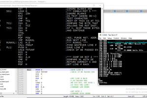
Hi! Yes, Cosmac is really a paragon of simplicity even now, my implementation is totally the opposite but it was done for learning and illustration of reimplementing existing CPUs using my microcode tool chain. In the meantime I improved elements of that and the microcode here could be improved too. If you decide to re-implement, feel free to reach out! Good luck!

  Are you sure? yes | no

John Jacobs wrote 05/30/2022 at 19:23 point

Wow. This caught my. My first introduction to computers was the COSMAC Elf. I had that as a working computer using my ELF and FORTH. I always loved the simple but effective architecture. Your choice of the 1802 hints you had the same experience. Could have easily been sped up. 

I am going to have to reproduce this project, when I can, to try it.

My second system was 6809 based CoCo. That was an innovative processor for the time period. 

  Are you sure? yes | no

Similar Projects

Does this project spark your interest?

Become a member to follow this project and never miss any updates