 EtchedPixels
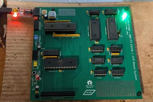
The 80C188 has a 20pin multiplexed address/data bus, and various lines don't quite work the way the Z80/RC2014 bus expect them. The bus is demultipliexed by a 74HCT373 and a 74HCT573 (same thing different pinouts). U3 also latches the S2 status line from the processor to ascertain if it should generate a memory or I/O cycle. A19 is then inverted by U4A because the standard linear memory 512K/512K card puts the ROM at the bottom as it was designed for Z180.
Other bits of U4 invert the interrupt signals as the CPU expects them to go high on an interrupt.
A pair of can oscillators drive the clocks. The first a fixed 1.8MHz into TMRIN1 so that all boards can have the same timer clocks, the second dependent upon the CPU speed drives the system clock to the CPU and it in turn drives the CLK signal on the RC2014 bus.
No provision is made for anything clever like an FPU.
 Jason Westervelt
 Tom
Tom
 Dave Collins