 Anool Mahidharia
Details
FAQ
This course consists of 4 pre-recorded videos and 4 live office hours. More FAQ here.
Classes are pre-recorded and will be released Tuesdays at 19:00 IST/9:30a EDT/ 6:30a PDT. Office Hours are Fridays at 20:30 IST/11:00a EDT/ 8a PDT. Link to calendar for easy timezone conversion.
ABOUT THIS COURSE
This “Introduction to KiCad and FreeCAD” course will consist of byte sized pre-recorded video tutorials which will walk you from schematic capture onward to PCB and enclosure design. In recent years, the line between hobbyist and professional has blurred. Hobbyists are designing and assembling circuit boards with grain sized components on multi-layer boards and dense parts placements. And thanks to rapid prototyping, modeling enclosures to house the electronics it pretty easy as well. To become a skilled hobbyist / professional, it is essential to have these design skills. But EDA and CAD tools have a very steep learning curve, and its not easy to get started unless you have a lot of guidance along the way. So, join in, and improve your engineering chops by becoming proficient in PCB and mechanical design.
Why KiCad?
KiCad is an amazing Open Source (free as in freedom!) program that allows you to design your own printed circuit board without arbitrary limitations on board size. KiCad offers an all-in-one solution:
- Full featured EDA suite, GNU GPL license
- Cross-platform - Linux, Windows, Mac OSX
- Large, dedicated support community.
- Extensive Documentation, FAQ's, Mailing List, Tutorials, IRC
Why FreeCAD?
FreeCAD is an open-source parametric 3D modeller made primarily to design real-life objects of any size. Parametric modelling allows you to easily modify your design by going back into your model history and changing its parameters.
WHO IS THIS COURSE FOR ?
This course is tailored for the electronic enthusiast who has just started off using KiCad or wants to switch to it from other tools. We will walk through a design from Schematic to Gerbers and answer your “how-to” questions.
Later, we will have a quick introduction to FreeCAD, learning how to model an enclosure after importing a 3D model of the finished PCB.
All you will need is a basic understanding of electronics and mechanical modelling.
COURSE CONTENT
Here’s how we will progress over the next four weeks.
Week 1 :
Essential KiCad links, discuss KiCad best practices, setup a project directory tree, do a schematic capture, understand symbol library management and create custom symbols
Week 2 :
Symbol<>Footprint association, essential PCBnew plugins, PCB layout, footprint library management and creating custom footprints, adding non-technical layers to help production and assembly
Week 3 :
Engineering/Manufacturing outputs - GERBERS, vector graphics, 3D CAD formats. BoM management, creating and adding graphics such as logos to the PCB
Week 4 :
Essential FreeCAD links, FreeCAD basics, essential workbenches, unifying KiCad and FreeCAD via the KiCad StepUp tools workbench, PCB import, simple enclosure design, Exporting for manufacturing
PREREQUISITES
On your Person, all you need installed is some basic electronics and engineering knowledge, and some drawing skills.
On your computer, you will need to install the two programs, along with some add ons.
- KiCad ver 5.1.6 : https://kicad-pcb.org/download/
- KiCad Libraries : https://kicad-pcb.org/libraries/download/
- Schematic, Footprint, 3D models, Templates
- KiCad Addons
- KiCad StepUp Tools : https://github.com/easyw/kicadStepUpMod/
- Interactive HTML BoM : https://github.com/openscopeproject/InteractiveHtmlBom
- FreeCAD ver 0.18.4 : https://www.freecadweb.org/downloads.php
- FreeCAD workbenches : KiCad StepUp Tools, Exploded Assembly, Fasteners, Manipulator, Sheet Metal
- To activate Workbenches, go to TOOLS > ADDON MANAGER
Course Classes
Collapse
-
KiCad + FreeCAD Class 1
Lutetium • 07/07/2020 at 16:54 • 0 commentsHere is the link to watch Class 1.
In this class, we cover:
00:00:32 - Schematic walk through
00:03:28 - Project Manager overview
00:05:05 - EEschema, toolbar review
00:12:00 - Start schematic process
00:13:20 - Place parts
00:18:50 - Place wires / connections
00:21:35 - Place Net labels
00:45:00 - Hierarchy Sheets
00:55:55 - ERC and Power Flags
01:00:30 - Libraries - backup, create, edit parts
01:09:55 - Wrap up Session ISee you in the Office Hours Friday!
-
KiCad + FreeCAD Class 1 NOTES
Anool Mahidharia • 07/07/2020 at 18:47 • 2 commentsAdditional Notes for Session 1 : KiCad + FreeCAD
GIT REPO
Here's a link to my GIT repo for review.
https://github.com/wyolum/HackadayU_KiCad_FreeCAD
VIEW FOOTPRINT IN SCHEMATIC LIBRARY BROWSER
In EEschema Library Browser, if you see only the schematic symbol but not the footprint, check this setting :
PREFERENCES > PREFERENCES > Eeschema > Show footprint previews in library browser (check)USE REPETITION FOR SPEED
If you have a bunch of repetitive actions to be done, such as placing incremental net labels, or the same length of wire connected to a succession of pins on an IC, then
- Set up Repetition parameters in
PREFERENCES > PREFERENCES > EEschema
- Set Horizontal pitch of repeated items
- Set Vertical pitch of repeated items
- Place the first item (net label, wire etc).
- Hit the “Insert” key and the item you placed will be repeated according to the parameters set in Preferences. If it’s a Net Label, it will also increment each time you “Insert”.
- Here’s a short video showing how it works.
BUSES
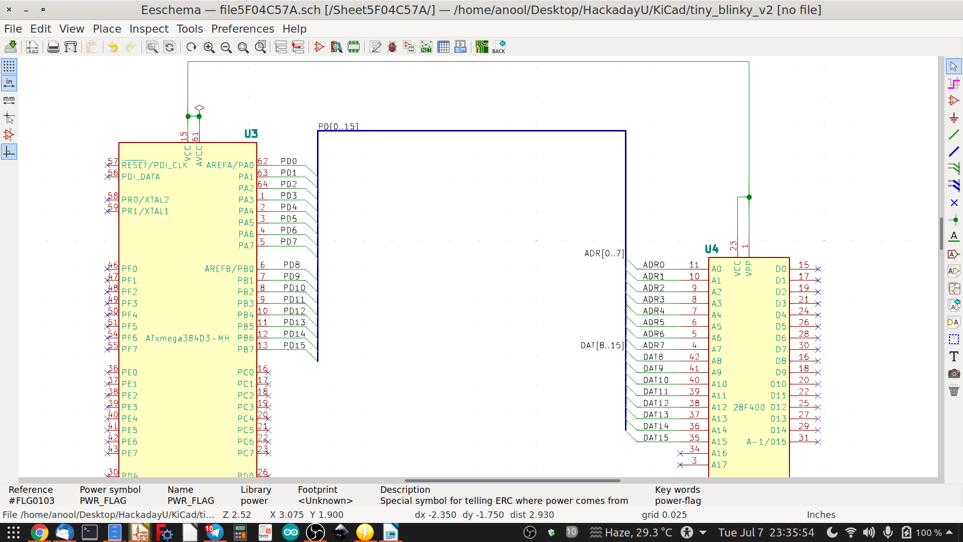
We looked at a super simple example of how busses can be used, it wasn’t exactly an appropriate use of the feature, since the same result can be achieved just by using Net Labels. But for example, if you have a more complex circuit, where there is a 16-bit data bus on a micro-controller labelled PD0..PD15, that needs to be connected to a memory device with 8 pins labelled ADR0..ADR7 and the other 8 pins labelled DAT8..DAT15, then the BUS feature solves the problem.
- Add wire stubs and bus entries on the first device (use the repetition feature to speed things up).
- Add wire stubs and bus entries on the second device
- Add net labels on the first device – PD0 to PD15
- Add net labels to the second device – ADR0 to ADR7 and DAT8 to DAT15
- Draw a bus that connects all of these pins
- Add a net label near the first device – PD[0..15]
- Add a net label near the second device – ADR[0..7]
- Add a third label near the second device – DAT[8..15]
The pins then get connected like so :
PD0 > ADR0
PD1 > ADR1
.....
PD7 > ADR7
PD8 > DAT8
PD9 > DAT9
.....
PD15 > DAT15
Here's a screenshot of how that looks
![]()
IGNORE SCHEMATIC SYMBOL
If you'd like to add a symbol on the schematic which should not be placed on the PCB, then add a "hashtag" to it's REFERENCE (example - #U4 instead of U4, and it will not be put on the PCB)
This can be used to show where off-board parts such as a Motor, Fan, Solenoid etc connect to a screw-connector on the board, for example.KiCad CHEAT SHEET
Handy KiCad cheat sheet for reference, in several languages
https://github.com/KiCad/kicad-doc/tree/master/src/cheatsheet
And here's the link to the KiCad forum if you'd like to give feedback to the author
https://forum.kicad.info/t/cheatsheet-for-kicad/5247 - Set up Repetition parameters in
PREFERENCES > PREFERENCES > EEschema
-
KiCad + FreeCAD Class 2
Anool Mahidharia • 07/13/2020 at 19:12 • 0 commentsHere is the link to watch Class 2.
In this class, we cover :
00:00:00 - Session II Overview and Session I review
00:04:15 - Bitmap to Component converter
00:09:40 - Symbol - Footprint association
00:15:20 - Create footprint library and import/add custom footprints
00:17:50 - Netlist Export
00:18:50 - PCBnew Toolbar review, layer manager, page, board and grid settings
00:25:10 - Netlist / Parts Import
00:28:00 - Parts - move, rotate, flip, place
00:34:10 - Board outline / Edge cuts
00:43:00 - Routing / Track layout
00:43:40 - Net classes setup
00:53:45 - Zone / Pour / Fill
01:02:45 - 3D View
01:03:05 - Silk and Fab Layer cleanup
01:10:15 - ERC
See you in Office Hours on Friday - note the revised time - at 20:30 IST / 11:00am EDT / 8:00 am PDT.
Link to calendar for easy timezone conversion.
I've updated the Git repo to reflect what we've covered in Session 2.
If you have any questions, please let me know here. -
KiCad + FreeCAD Class 3
Lutetium • 07/20/2020 at 19:10 • 0 commentsHere is the link to watch Class 3.
In this class, we cover:
00:00 Intro
02:20 Dimensions, Origin offsets
05:30 Interactive Routing
06:55 Modify edge cuts
10:15 Archive footprints in custom library and swap references
16:15 Keepout Areas, Exposed zones
23:45 Plugins
31:20 Interactive BoM
33:20 Plotting - Gerbers, Position files and PDF's
39:45 GerbView
42:30 Export - STEP and VRML
46:30 Create custom footprint and add to project library
55:20 Back import
57:00 Add 3D model for custom footprint
59:55 Interactive Routing - Advanced features -
KiCad + FreeCAD Class 2 Q&A
Anool Mahidharia • 07/21/2020 at 20:15 • 0 commentsClass 2 Office Hours Q&A:
Here are the Questions (and answers) from the Class 2 Office Hours Q&A
- What exactly is this project that we’re designing? What might it be able to do?
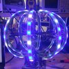
- Functionally, not very specific. I had to choose something where I could demonstrate as many features as possible. Having said that, this drives the RGB LED’s, so it can be used as a Badge, or a trinket. I’m not covering the programming, but loading the Arduino bootloader, and then running the NeoPixel demos should get it to light up
- Doing some Googling, I found these couple of projects (there’s likely many more) that use the ATtiny85/WS2812B combo.
- https://www.instructables.com/id/Use-a-1-ATTiny-to-drive-addressable-RGB-LEDs/
- https://www.electromaker.io/blog/article/programming-ws2812b-leds-with-attiny85-23
- Was there a reason to place the Neopixels closer to the edge of the board instead of the mounting holes? I would think that placing the mounting holes closer to the corners would be preferable.
- The plan is that when we make the enclosure in FreeCAD, the main circuit board (area within the mounting holes) can be enclosed, while the part with the RGB LED’s can stick out / be exposed.
- If in-case, my logo size or the layer is wrong, how do I change those parameters?
- There’s no easy way, other than going back to Bitmap to Component converter, and regenerating the symbol / footprint all over again.
- I’m pretty bad with electronics. I notice that between the end of Class 1 and the start of Class 2, the schematic has changed, which is throwing me off, because I don’t know the missing steps that got from version 1 to version 2. Specifically, I now see a box around the connectors at the end of the LED chain. But, more importantly, when I was watching you assign footprints, you have a “5V” (J4) that I do not have…
- UPDATED: I’m guessing you customized the connectors to add boxes around them. And changed the power supply, changing the female connector to male, and adding a female connector between the end of the Class 1 and the beginning of Class 2.
- Yes, sorry about that confusion. Anyhow, I’m posting my project files on Github, so you can clone that repo, and compare.
- https://github.com/wyolum/HackadayU_KiCad_FreeCAD
- My default in Board setup is quite different from yours. (I’ve never used it before, so this is what it installed with):
Clearnc
Track Width
Via Size
Via Drill
uVia Size
uVia Drill
dPair Width
dPair Gap
0.2 mm
0.25 mm
0.8 mm
0.4 mm
0.3 mm
0.1 mm
0.2 mm
0.25 mm
UPDATED: I did not know mil as an imperial unit. I see now that the above values are the metric equivalents -- or close to -- the mils shown in your defaults.
- Try changing the project “Units” to INCH instead of MM. In Schematic/PCBnew, the second and third toolbar icons toggle between these two.
- Then, in PCBnew > BOARD SETUP > DESIGN RULES > NET CLASSES , you can set it up. I’m posting my project files on Github, so you can clone that repo, and compare.
- https://github.com/wyolum/HackadayU_KiCad_FreeCAD
- In Board Setup, when you are changing the widths of the routing, I see you have /A1, /A2, /A3, /D1, and /D2. Mine does not have those labeled that way. When / how did that happen?
- I wanted to show how the BUS function works, so I made some changes to make that clear and renamed the nets. Actually, I made some more changes, so best to clone my version from the repo (see link above) and let me know if you need help to replicate my version.
- My SPI PROG footprint is “backwards” with pins 1, 3, and 5 at the top. I hope the right thing to do was to mirror it in the Footprint Editor, save as tiny_blinky, update the Symbol Fields in Eeschema, and change the footprint in Pcbnew… It now looks like yours…
- Ummm, Prolly. Did you try ROTATE / MIRROR / FLIP (X/Y) options within Schematic itself ? Maybe if you share a screenshot, we can sort it out.
- What exactly is this project that we’re designing? What might it be able to do?
-
KiCad + FreeCAD Class 3 Q&A
Anool Mahidharia • 07/24/2020 at 17:48 • 0 commentsClass 3
- When setting the origins, how close is “close enough”? The center of my board, mathematically is 1.4375 inches by 0.8 inches. However, the closest I could get seemed to be 1.4350 (or 1.4400) inches by 0.8 inches. (ubuntourist)
- Set your Grid Size to 25 mil instead of 50 mil
- OR
- Block Select All (make sure to enable all layers first) > Secondary click > Move Exactly (hotkey ctrl + M) , set X coordinate to -0.0375 > OK
- This’ll move the board to X=1.4 and Y = 0.8
- Racing to finish… Still 15 minutes left in the video. I see your Oshpark display of your part is much more detailed than mine… I mean, the detail that I see in the files that I’ve zipped up and submitted gets lost in translation… (ubuntourist)
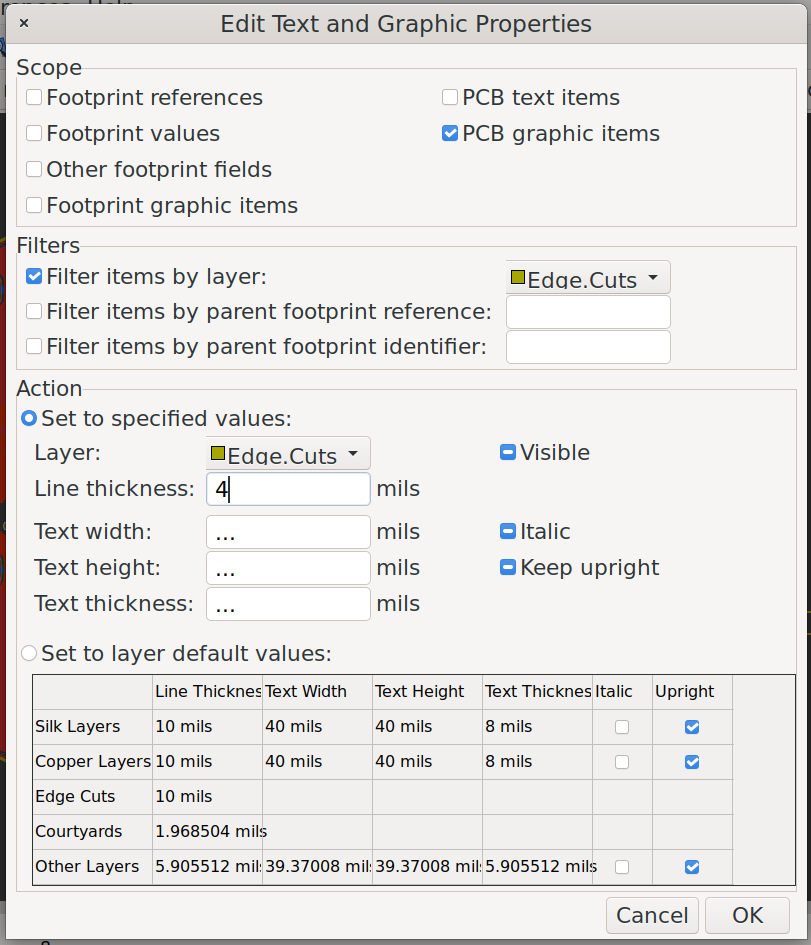
- Well, WYSIWYG,
- Ah, gotcha. I know what that is. I ran into this error last week, and have a temporary fix until OSHpark fixes it. If your edge cuts layer line thickness is less than 4 mil, OSHpark render fails. If the line thickness is 4 mil or more, it works.
- Make sure your Board Edge Cuts layer graphics thickness is at least 4 mil or more.
- Go to EDIT > Edit Text and Graphics Properties, (see image below)
- I am getting an error while creating the step file. It says “Unable to create STEP file. Check that the board has a valid outline and models.”......... I have already drawn it three times...any tips to avoid the error in the future or any idea how I can debug the current edge cut of the board?
- Error is what it says - the board outline has a discontinuity. Sometimes, if the discontinuity is large enough, KiCad will complain when you try 3D view.
- If discontinuity is very minute, 3D will work, but STEP will fail
- Fix your Edge Cuts layer graphics to fix this. There should not be any discontinuities in the outline. This usually occurs if you have set a very fine grid size (such as 1 mil instead of 10 mil), and the end points of two consecutive elements do not line up and are not coincident.
- In my KiCAD installation, my right-side toolbar doesn’t show all the functionalities like in the video. How can I adjust the toolbars. I faced this problem both in Eschema and PcbNew. I searched online but didn’t find anything.(Aditya)
- Can you post a screenshot ? What parts are you missing ?
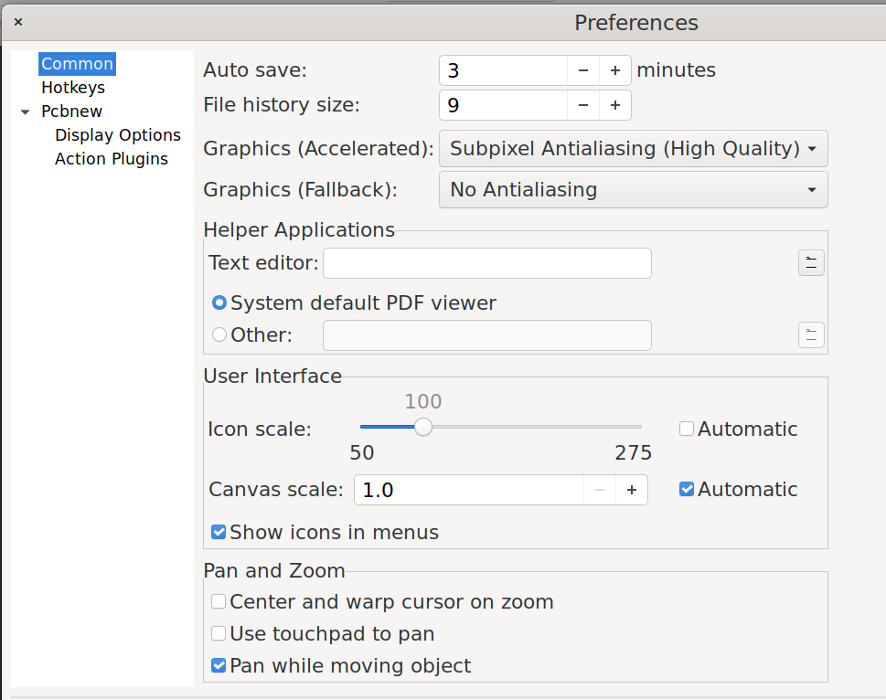
- Looks like ICON scaling issue.
- KiCad > PCBnew > Preferences > Common > User Interface > Icon Scale
- Also, when we do the pcb page setup, how do you decide which layers you need or don’t need?(Aditya)
- Depending on number of copper layers, you need
- all the copper layers
- Top/Bot Mask
- Top/Bot Silk
- Edge Cuts
- .DRL drill file
- For getting a solder paste Stencil made, you need
- Top/Bot Paste
- For board assembly you need
- .POS files (FILE > Fabrication Output > Footprint Position Files
- Top/Bot Adhes (adhesive) - but not always necessary (most board houses auto-generate this from the other layers)
- Top/Bot Fab (fabricate) layers can be helpful too, in addition to 3D images in various orientations for visualisation
- This is a bit off the class scope. I came across the PCB Motors on Hackaday’s blog last year. They were made by Carl Bujega. I noticed on his youtube channel that he uses Altium to not just design PCB motors, but also flexible PCBs. I wanted to know if something similar to that is possible to replicate on KiCAD.
- Rigid or Flex PCB is not a problem at all - as far as KiCad is concerned, the only difference is in the board thickness, everything else stays the same.
- But you may need extra plugin’s to design helical coils and such for the motor “windings”. Just look for appropriate plugins as needed.
-
KiCad + FreeCAD Class 4
Anool Mahidharia • 07/29/2020 at 19:04 • 0 commentsHere is the link to watch Class 4.
https://www.youtube.com/watch?v=lbnrUtgFFCc
In this class, we cover:
00:00:08 - Session Overview
00:00:20 - FreeCAD walk through, Preferences, Addons and Addon Manager, Customise workbenches
00:03:05 - Part workbench, working with primitives
00:04:00 - Navigation, mouse control
00:09:00 - Sketcher Workbench
00:17:00 - Part Design workbench
00:26:00 - KiCad StepUp Tools workbench - Edge Cuts layer push / pull
00:38:00 - KiCad StepUp Tools workbench - PARTS push / pull
00:46:45 - STEP model manipulation
00:56:50 - KSU WB Footprint / 3D model alignment and export
01:04:10 - Review, Part workbench Shape Binder quick overview, Session wrapup -
KiCad + FreeCAD Class 4 Q&A
Anool Mahidharia • 07/30/2020 at 14:45 • 0 commentsClass 4
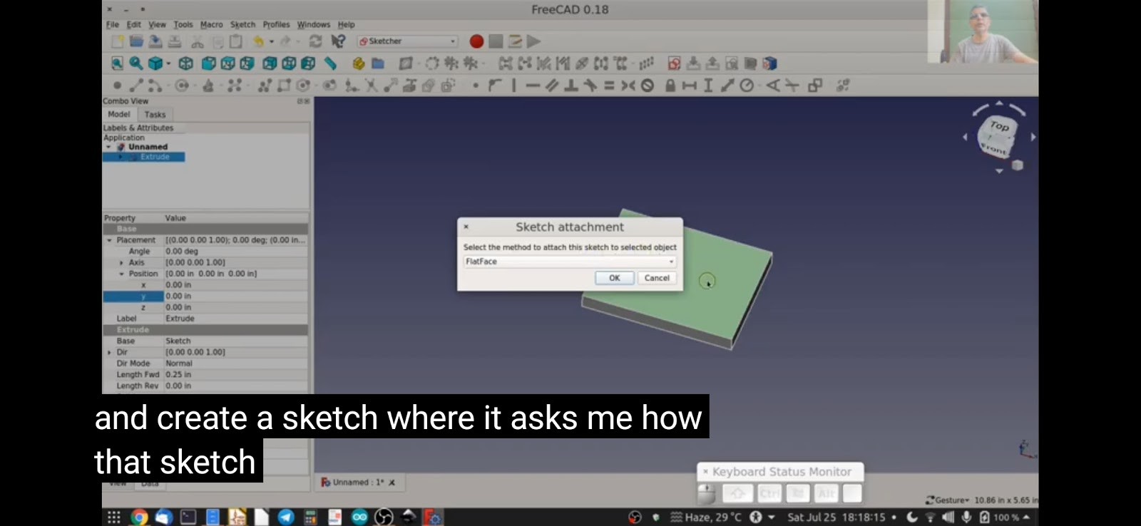
- At 14:39 in the video, after constraining the internal rectangle sketch, while you are still in the sketch workbench, your video shows the outline sketch (Sketch001) on the top face of the Extrude part. I cannot see that in my version. All I see is the Extrude part, even though the Combo View shows me all the data and view information for both Extrude and Sketch001. The sketch lines are invisible. How do I make it visible?
- What do you see in the wireframe mode? Did you select top face of "extrude" first, then start the second sketch, making sure you use "sketch attachment - flat face" ?
- Yes to both questions. See https://codeberg.org/ubuntourist/Tiny_Blinky/src/branch/main/class_4_14:39_broken.FCStd
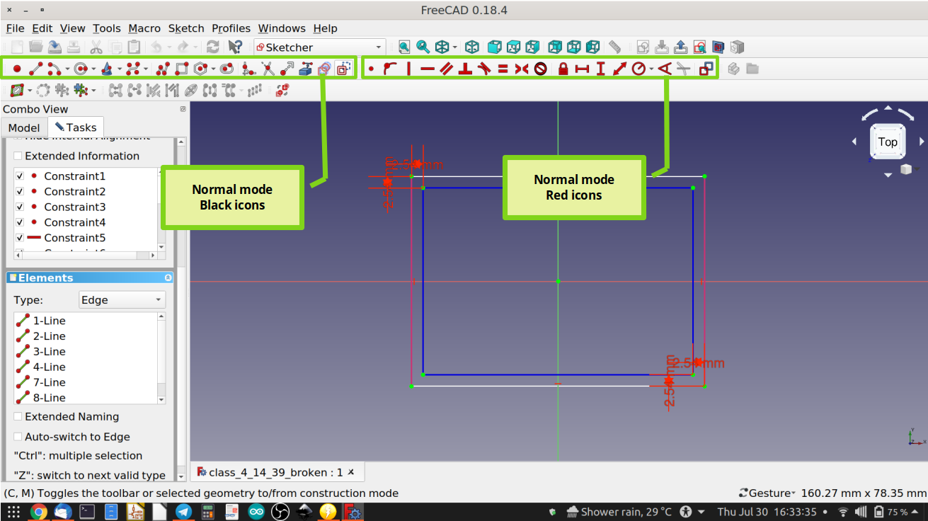
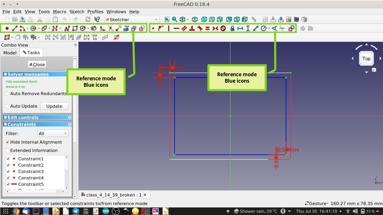
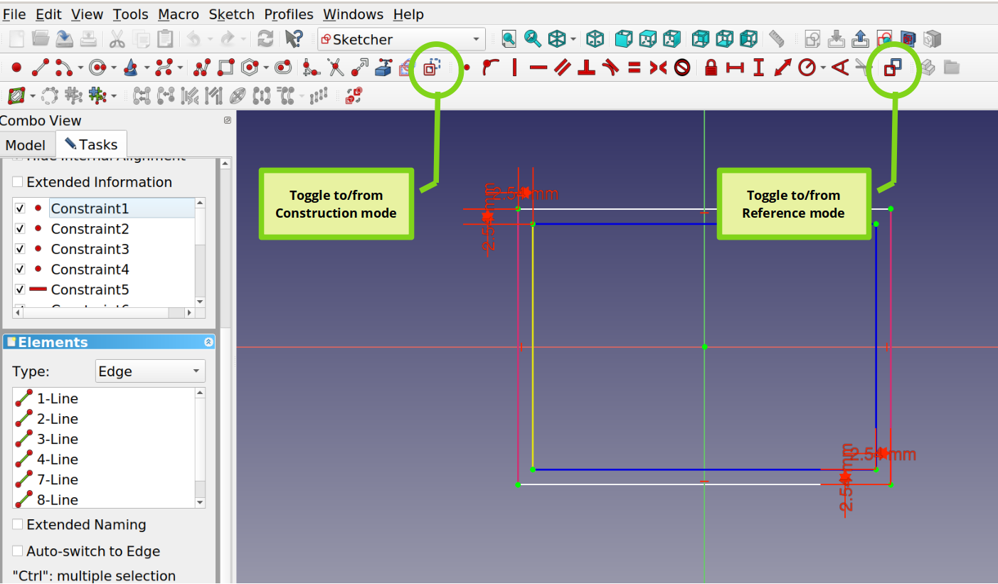
- Ah, I see the error in the file link you sent me. The sketch you have drawn shows up in line color “blue”. This means those four lines of sketch001 are “construction lines” - which I didn’t cover in the video. Construction lines are drawing aids you use to help make sketches, but which are not part of the real sketch. So think of them as “virtual” reference elements to help you create a sketch. To toggle between regular sketching and virtual “construction mode” sketching, use the last icon in the Sketcher “drawing tools” toolbar.
- Ah. Done. Thanks.
![]()
![]()
![]()
![]()
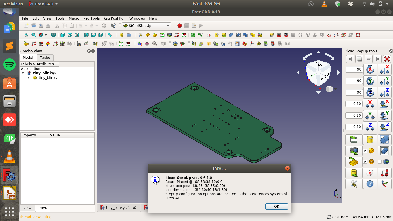
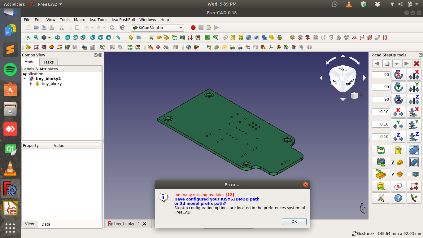
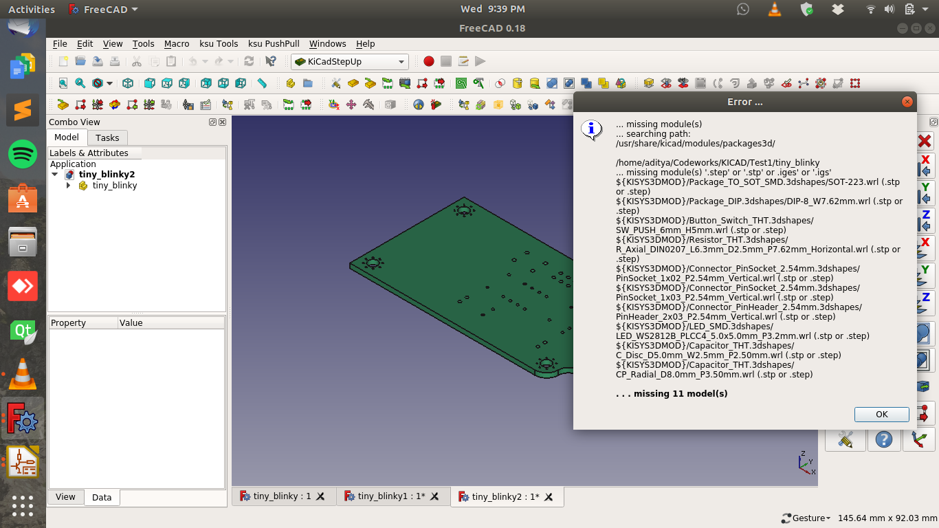
- Sir, when I am trying to import the kicad_pcb file, only the base board loads up. I am giving the screenshots of the error messages. Also I verified the 3D package path and it’s correct in both KICAD and FreeCAD.
![]()
![]()
![]()
Your KISYS3DMOD needs to be usr/share/kicad/modules/packages3d- Make sure you’ve set this correctly in KiCad and in FreeCAD KiCadStepUp tools Preferences.
- Make sure you have the latest library downloaded from the KiCad github repo.
- Use this URL : https://github.com/KiCad/kicad-packages3D
- It’s likely you’re missing all the models. For example, search for SOT-223.wrl and SOT-223.step (or SOT-223.stp) - you ought to have both available in the “Package_TO_SOT_SMD.3dshapes” folder.
-
LINKS
Anool Mahidharia • 07/30/2020 at 18:54 • 1 commentAdding all links in a single Project Log - work in progress.
If you spot a mistake or there's a missing link, please let me know.
PROJECT
- Project repository : https://github.com/wyolum/HackadayU_KiCad_FreeCAD
PROGRAMMING
If you physically build this project, here are some links you can use to figure out how to program the ATtiny
- https://www.instructables.com/id/Use-a-1-ATTiny-to-drive-addressable-RGB-LEDs/
- https://www.electromaker.io/blog/article/programming-ws2812b-leds-with-attiny85-23
- https://www.instructables.com/id/Program-an-ATtiny-with-Arduino/
- https://create.arduino.cc/projecthub/arjun/programming-attiny85-with-arduino-uno-afb829
KiCad
- KiCad ver 5.1.6 : https://kicad-pcb.org/download/
- KiCad Libraries : https://kicad-pcb.org/libraries/download
- KiCad Schematic Symbol Libraries : https://github.com/KiCad/kicad-symbols
- KiCad PCB Footprint libraries : https://github.com/KiCad/kicad-footprints
- KiCad 3D models : https://github.com/KiCad/kicad-packages3D
- NOTE : For Mechanical CAD integration with FreeCAD, 3D models must be available in STEP format. KiCad can use either STEP or WRL formats. WRL export produces "better looking" results, but is not suitable for manipulation in FreeCAD. STEP export works with FreeCAD but loses information such as textures, shininess, transparency etc.
- KiCad Project Templates : https://github.com/KiCad/kicad-templates
- KiCad Cheat Sheet : https://github.com/KiCad/kicad-doc/tree/master/src/cheatsheet
- KiCad Plugins
- Teardrops : https://github.com/NilujePerchut/kicad_scripts/tree/master/teardrops
- Circular Zones and Via Stitching : https://github.com/jsreynaud/kicad-action-scripts
- RF Tools : https://github.com/easyw/RF-tools-KiCAD
- consists of Rounder for tracks, Solder Mask Expander, Track Length, Via Fence Generator
- Interactive HTML BoM : https://github.com/openscopeproject/InteractiveHtmlBom
- Plugins from External Tools link at KiCad : https://kicad-pcb.org/external-tools/
- Curated list of KiCad 3rd party tools : https://github.com/xesscorp/kicad-3rd-party-tools
- KiCad CHEAT SHEET : https://github.com/KiCad/kicad-doc/tree/master/src/cheatsheet
- KiCad FORUM : https://forum.kicad.info/t/cheatsheet-for-kicad/5247
FreeCAD
- FreeCAD : https://www.freecadweb.org/downloads.php
- FreeCAD Addons : https://github.com/FreeCAD/FreeCAD-addons/
- FreeCAD Macros : https://github.com/FreeCAD/FreeCAD-macros/
- FreeCAD - Recommended addons :
- FreeCAD GETTING STARTED : https://wiki.freecadweb.org/Getting_started
- FreeCAD FORUM : https://forum.freecadweb.org/
3D CAD MODELS
- 3D Models : https://www.3dcontentcentral.com/
- 3D Models : https://grabcad.com/
- CAD file format converter : https://cloud.cadexchanger.com/
Enjoy this course?
ShareDiscussions


I searched them also and I found it: https://github.com/Ekran/HackadayU_KiCad_FreeCAD

Know anything about "the competition" -- Horizon EDA (https://horizon-eda.org/)?
I found it whilst stumbling around looking for something else.
In my near complete ignorance, it looks "interesting" and seems to have been getting recent love in terms of continued development work but I don't know if there's any real buy-in from the community.

Saw it a while ago, but haven't had a chance to check it out yet. It's on my to-do list.

Hello Sir!
In yesterday's office hour, you mentioned you would put the links related to KICAD action-plugins and templates on this page. Could you please share the links? I would love to try out the amazing templates that you showed!
Will add a comprehensive LINKS project log, but in the mean time, here's a link to the Templates :
https://github.com/KiCad/kicad-templates
https://kicad-pcb.org/libraries/download/
HTH !
I would like to see one more class that talks about setting up Kicad with all of the footprints. I downloaded the footprints and installed them. But later I found out you appear to have to load them manually one at a time?
When the board was completed in Class 2 I did a 3D view of my board and the Capacitors were drastically larger than what their footprint in 2D shows. I'm sure it had something to do with mapping the 2D footprint to the correct 3D footprint.
In my footprint library I see Capacitor_THT.pretty and Capacitors_THT.pretty. When I added my capacitors I used the Capacitors_THT reference. I later noticed that you used the Capacitor_THT reference...so I changed it. But still no luck. The 3D view shows the wrong size capacitors.
Everything else looks OK. I'm just a bit lost as to why my libraries are so screwed up. The class time at 8am on Friday is bad for me. I have a meeting every Friday for work.
Perhaps you can add this to the 1st class in the August time slot, i.e. the 2nd round for this class. I will gladly sign up again to get more information. Your class is awesome.
Thanks for the feedback. Have you done a fresh git repo clone of the libraries ?
Schematic symbols: https://kicad.github.io/symbols
PCB footprints: https://kicad.github.io/footprints
3D models: https://kicad.github.io/packages3d
Templates : https://github.com/KiCad/kicad-templates
I recommend you do a fresh download to an empty folder, and reassign the paths in KiCad for symbols, footprints and 3D packages.
If you can't attend office hours, just add you questions to the Q&A doc on Google [ https://docs.google.com/document/d/1oJc1sW4ZMSlCw0z1culPuzAjrDhr_zM8GoafmbaMEL0/edit ] and I'll add an answer.
The Q&A doc is also added to as Project log so everyone can check it out.

Hi everyone and thanks for joining us in Kicad + Freecad.
We provided the pre-recorded video in advance so that people could learn at their own pace. Sorry that wasn't clear in the ticketing site. Bear with us while we get this program off the ground. There will be a live Office Hours on Friday where you can ask questions.
-If you'd like a refund because you didn't get what you were expecting, please request one through the ticketing site.
-If you enjoyed the class, let us know!
-Feedback is welcome, superconference@hackaday.io.
Last night, I went through the tutorial and ended up with nice pretty PDF's of the schematics as shown in the video. (Took me bloody forever, since I'm very new to this and have zero electrical engineering chops.) But I'm religious about taking notes and have a nice README.md (and corresponding README.pdf) with my notes. Two questions / comments though:
According to dpkg I have kicad 5.1.6-202005120818+c6e7f7d~86~ubuntu20.04.1, which would seem to satisfy the "5.1.6" prerequisite. However, I noticed two differences:
1. When selecting a part from the symbol library, the video shows both a schematic image, and underneath that a... footprint? I think. Mine does not show the footprint thingie. Is that an option I can set or do I really need to download yet another non-integrated version of application? (I really hate doing that, and may just end up living without the preview.)
2. The other minor difference: When moving the ATtiny to make room for the bus, in the video, only the wires for pins 2 and 3 "broke". In my version, the pin 8 wire broke at the junction for the SW1 switch. Not a big deal. Just a comment.
Hi @ubuntourist , way to go !
1. In EEschema, can you go to PREFERENCES > PREFERENCES > EESCHEMA > Show footprint reviews in symbol chooser (enable)
2. That could be due to how the block was selected. Also, after selecting the block, did you choose "move" or "drag" ?
Thanks.
1. I looked but missed it the first time. I now have footprint preview enabled.
2. I chose "move"... I think. 😉
Also. One more quick question: I'm guessing that the downloaded symbols, footprints and packages3D include everything that was already in the stock Debian package. Yes?
(I downloaded and unpacked them a few weeks ago, but I didn't want to screw up the existing default paths "/usr/share/kicad/..." nor overwrite the files that are managed by dpkg. In any case, using the files in /usr/share/kicad/ seemed to work okay last night...)
Answer to your new Q - Yes,
I recommend cloning the three repos locally, and keeping them updated frequently.
But if "usr/share/kicad/.." works for you, then whatever floats your boat.
Unfortunately there is no live event, they just posted a pre-recorded YouTube video with a very, very bad quality. I hope they'll fix it on the next week.
I'm sorry you had an experience lower that your expectations. Do you have feedback that can help us improve ?
no one is starting the zoom meeting! Why? I've been waiting for more than 5 minutes.
I thought I had saved a link to the zoom meeting, but then could not find it anywhere, and assumed I must have seen it on a page that was later edited to remove it. I would not have gotten up so early had I known there was no live event.
Sorry about that, @ubuntourist !
We felt releasing a pre-recorded video will allows everyone to follow their own pace, instead of trying to keep pace with a live video. Anyhow, there's the live Q&A session scheduled for Friday.
Actually I think this way is better (pre-recorded videos instead of live sessions) but as Ubuntourist said, if you told us that the video was pre-recorded we wouldn't have gotten up that early, so please consider telling us with any new changes. One more thing, the audio & video quality was very bad, please try fixing them. Thanks.
So. The scheduled time of Tuesday 07/07 is more of a fantasy and I should just watch the YouTube videos, yes? Not anything "live" that I need to attend?

I kind of thought the live event was a Q&A hour on zoom or silent watching the stream with moderated questions, but to be fair the youtube videos are sufficient and very good, I imagine the comments section will become a goldmine of info.
Hi All,
We decided to release just the pre-recorded video so everyone can go through it at their own pace. And then on Friday, 10th, we will have the "live" Q&A session where I'll be available.
If you don't want to wait until then, feel free to ask either here or on the project "chat" messaging.
hello, I've spend about an hour trying to enroll to this course, can some one help please.
I'm a little confused about the signup process. I'm assuming I go to the Eventbrite link and sign up there. There are 4 dates listed and, the documentation states that I need to sign up for all four dates. So, I guess these are the 4 individual weekly progressive courses? And, if I need to sign up for all four, is there a way to aggregate them and checkout all four under one donation. Very painful if you have to checkout each individually.
Sorry about that. I wasn't aware how the sign up process works, but I can send the feedback to the team that handles this at Hackaday.
So. I've got the most of the prerequisites.set uop.. except I don't know where to unzip the three honkin' KiCad zip files. I'd rather not pollute anything put in place by dpkg.
Is there a common userland path where KiCad expects to find the unzipped footprints, packages3D and symbols?
If not, I'm inclined to try to make KiCad play like the other children and hang everything -- including the InteractiveHtmlBom plugin -- off of ~/.local/share/kicad/, adding a /footprints/, /symbols/ and /packages3D/ under that.
And then figure out how to set the environment variables or what-not to make KiCad find stuff there.
You can put them at any location, and then get KiCad to point to the appropriate path under PREFERENCES >> CONFIGURE PATHS
Will there be any hardware requirements beyond the computer?
("Cuz I ain't got any." 😜)
Hi! Thank you so much for doing this, I ran an intro kicad course in my workplace and at my school, let me know if there's anything I can do to help!
Thanks, Andrew. I've posted images of what we'll cover in the class, so maybe you can go over them to see if you spot anything amiss. The plan is to build a Blinky using an ATtiny85. A Github repo will be added sometime soon.
I have "some basic electronics and engineering knowledge" but not much... VERY basic, I would say.
Shouldn't be a problem at all. Between the videos and instructions posted here, you'll be able to pick it up. And we're here to answer any questions if you get stuck.

Thanks for doing this @Anool Mahidharia . Are there dates yet?
Working on it. Ought to be announced some time soon. There'll be a post on the Hackaday blog too announcing it.
KiCad 5.1! You'll soon be 3 versions behind. Either do a new course for KiCad 8 any day now or advise people a lot of stuff in this course is out of date.