 Noeël Moeskops
Apsu PCB Design
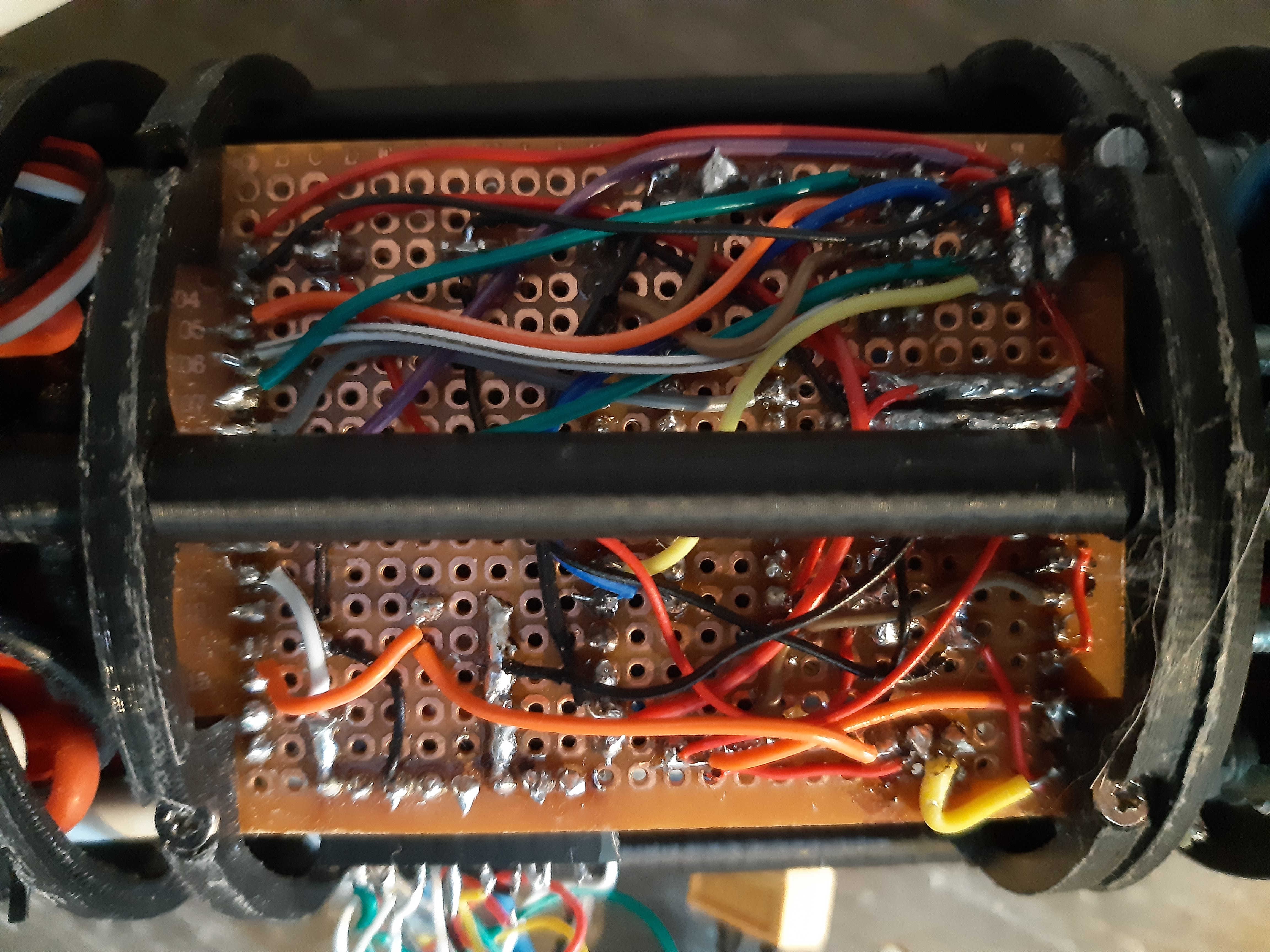
Since the beginning of the project I wanted to create a PCB that houses the electronics of the project. This was later further motivated by the big rats nest and space limitations of the prototype board I was using. Some wires kept going out mid dive duo to the 2.54mm pin-headers not being really movement friendly.
I also wanted to add extra sensors for finer movement control of the ROV. Because currently the device is blind and deaf to its surroundings. So it is required to do all the steering, calibrations and adjustments manually. I choice to fix it in my next iteration of the project by designing a PCB with the follow features:
- ESP32
- Inertial Measurement Units (IMU) (compass, gyroscope and accelerator meter)
- JTAG and UART debug ports
- expansion port for future additions
- RS485
- on-PCB temperate measurement
- water t temperate measurement
- battery and ESC temperate
- Humidity sensor
- outside pressure sensor
- inside pressure sensor
- BLHeli motor driver
- SimonK (PWM) motor driver
- 2xwaterlevel measurement
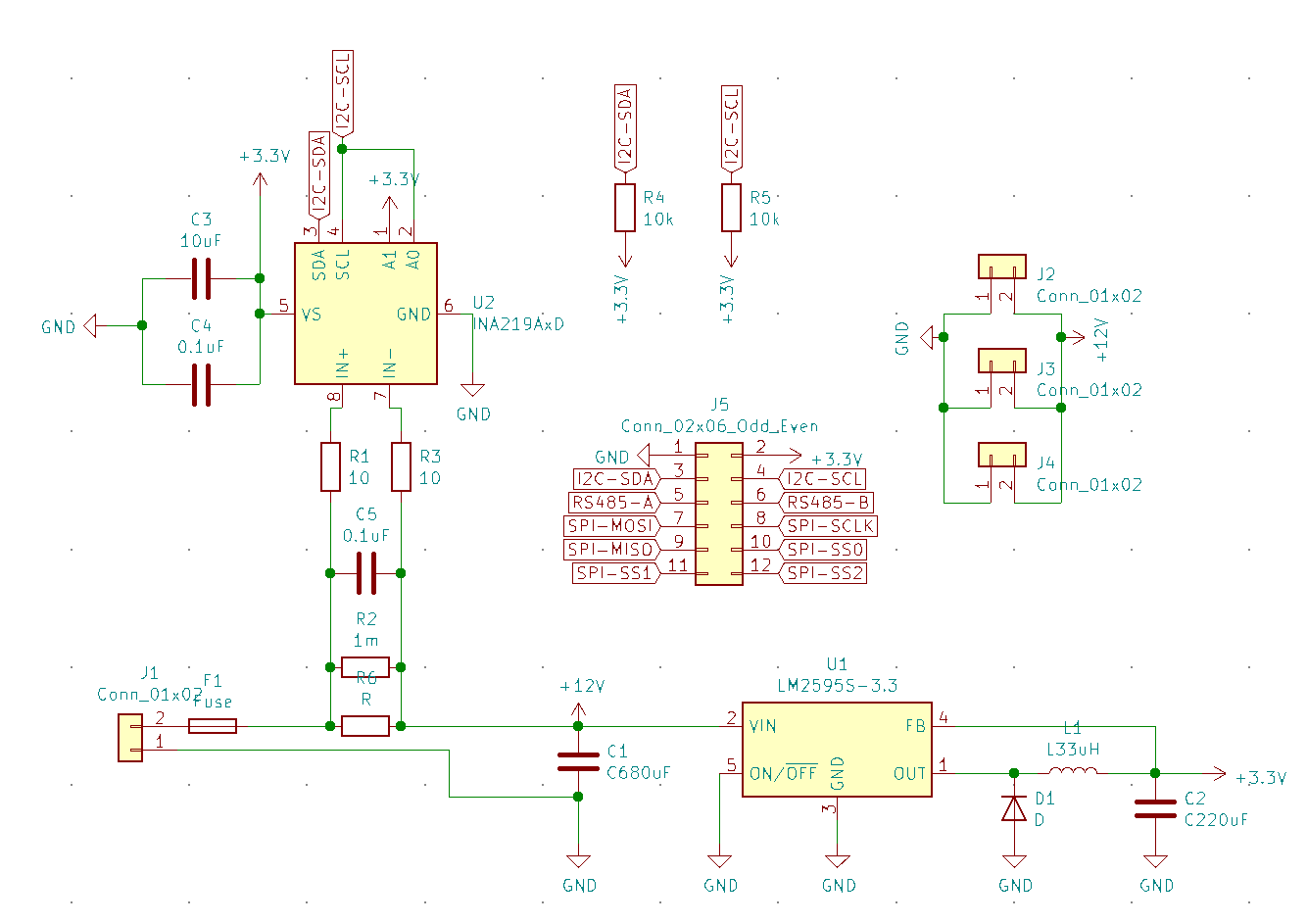
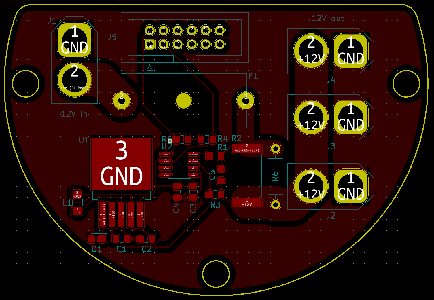
For all things concerning power I decided to create a separate PCB with:
- battery voltage measurement
- complete circuit current measurement
- XT60 breakdown
- 12V to 3.3V step-down
Here is a complete block diagram breakdown of the two PCB:
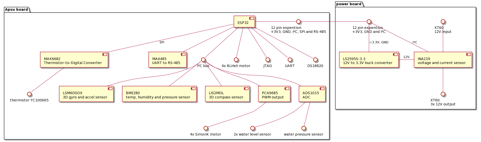
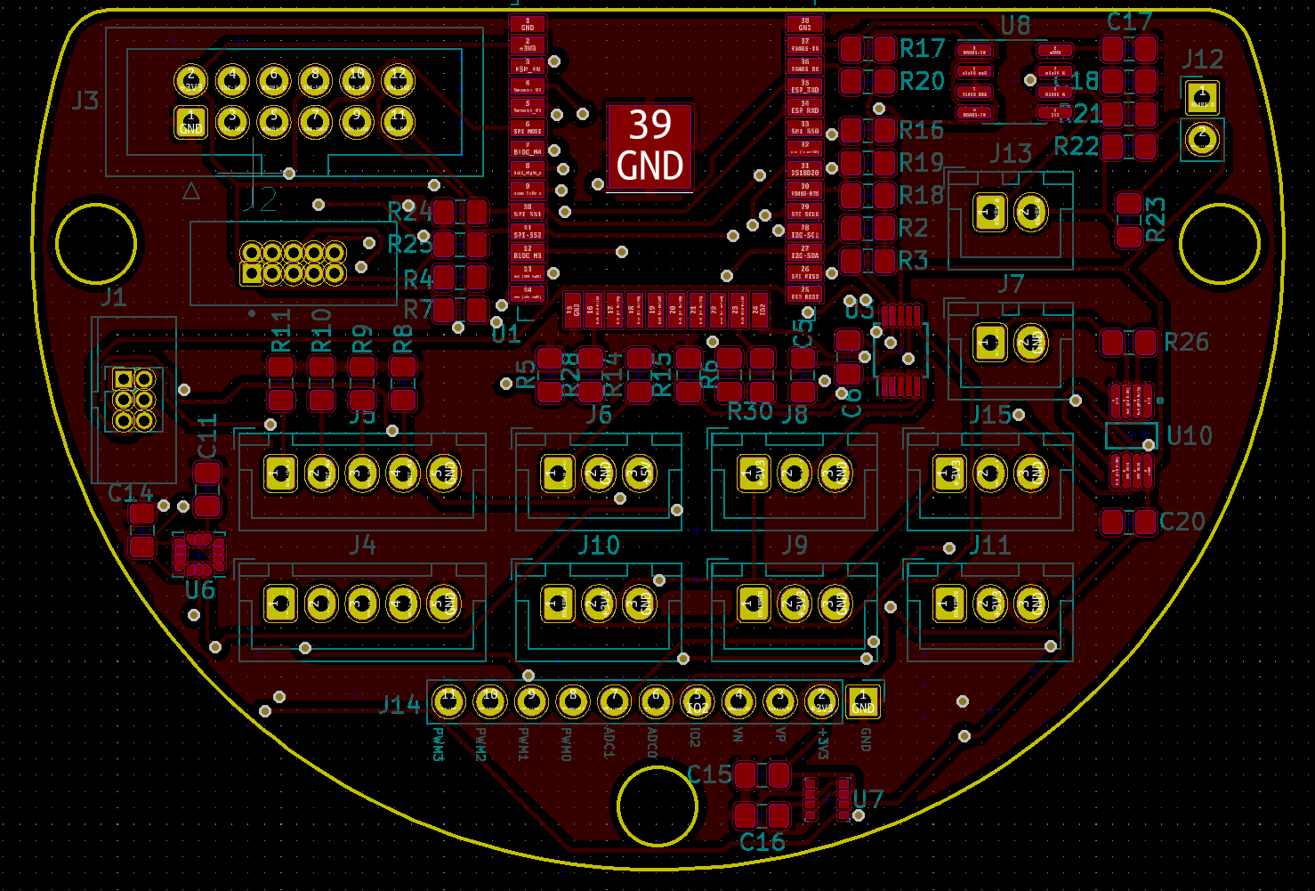
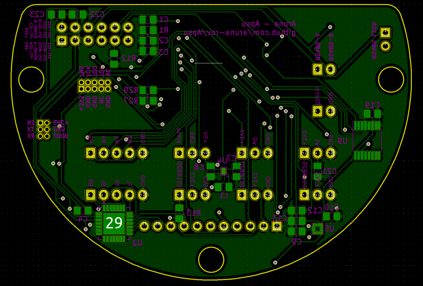
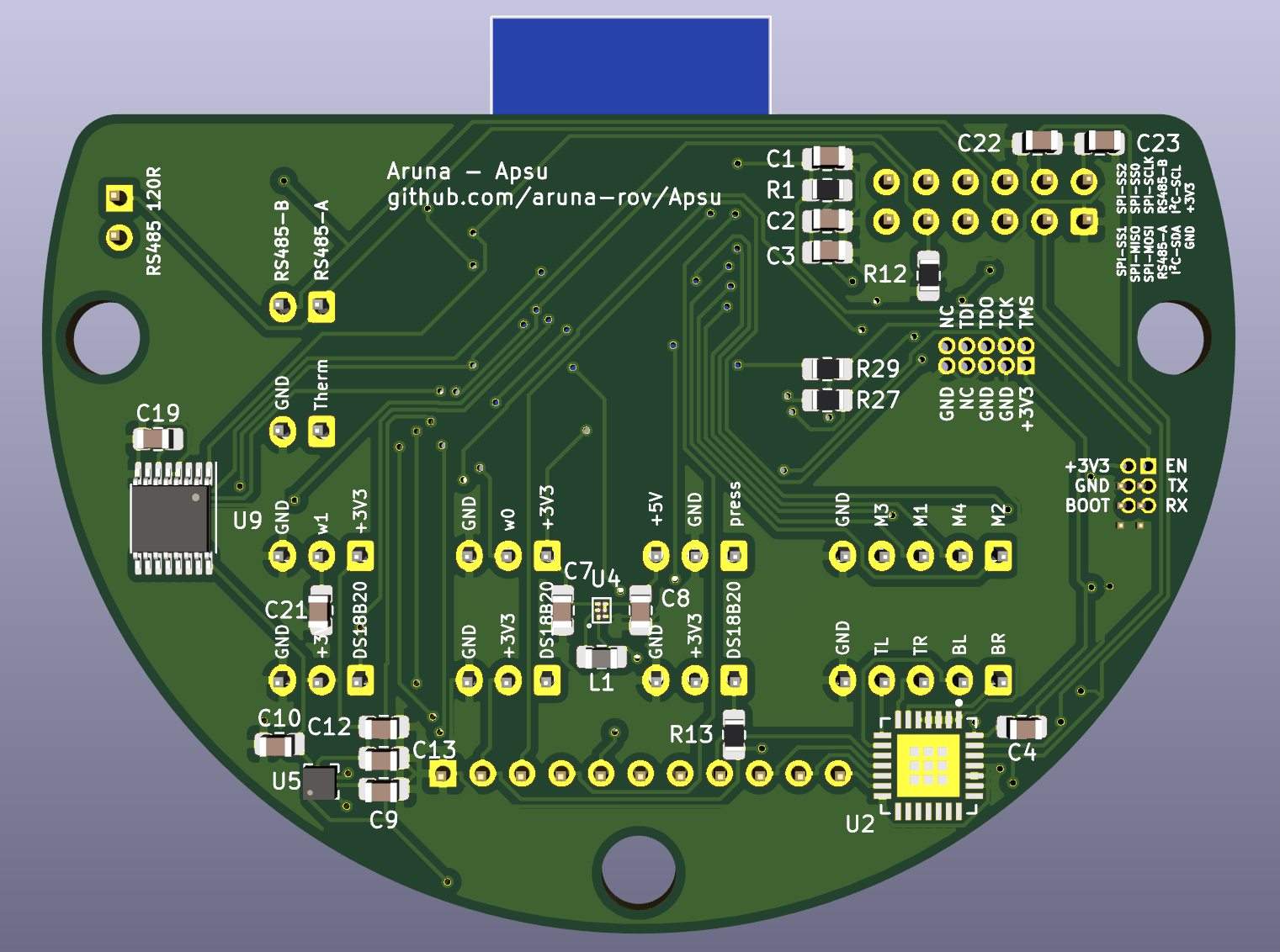
Apsu board
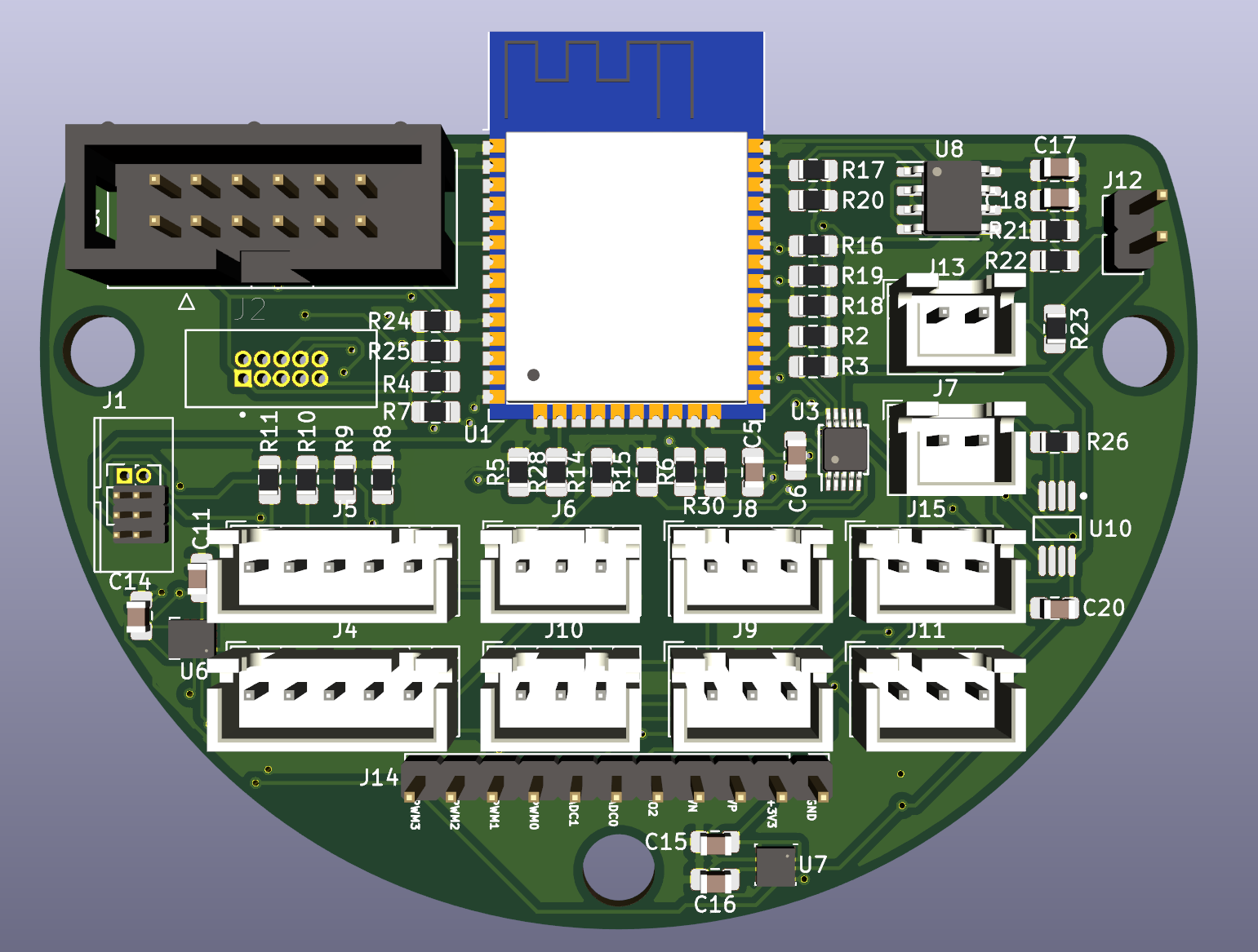
I originally wanted to create the board with a naked ESP32D (U1) chip, without the shell that contain the flash and a crystal and such. But I got intimidated by the data-sheet and the complexity that the ESP32 requires to operate. So as inexperience as I am, I decided to go with the ready to use ESP32-WROOM.
The IMU sensors are formed by an LSM6DOX (U6) made by IT controlled over I²C for 3D accelerometer and 3D gyroscope. The compass is also from ST; the LIS2MDL (U5) also controlled with I²C. Picking these chips was no easy task as I originally wanted to have the boards fully hand soldered. But IMU-type chips are rarely that big, so I instead went with the highest accuracy/price combination that was also highly available and well known to make it easier to write drivers for.
JTAG capabilities are of course an absolute must, especially since I have not yet created drivers for 90% of the IC’s attached to the ESP32. 1.27mm pin header (J2) where chosen because big 2.54mm simply would not fit.
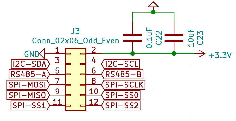
To keep the project modular I designed an expansion port that can daisy chain to as many boards as you want.
- GND and +3V3 to supply (and get) power to other boards
- I²C/SPI for peripheral master-slave communication
- RS485 for master-master communication
- SPI_SS0-2 for Slave-select, total of eight SPI slaves are supported. `0b0` is standard selected and `0b1` is in-use for the pressure sensor
RS485 is brought by a MAX485 (U8) chip, uses J13 for outboard A and B. short J12 if it's the end node to connect the 120Ohm resistor between A and B.
Temperature, Humidity and in-hull pressure is all measured by a BME280 (U7) by Bosh, communication over I²C. The humidity and in-hull pressure are used to detect hull breaches. Because the air pressure will rise when the hull is breached and the humidity will also rise. Having multiple redundant ways of measuring something critical as a hull breach is important as it increases safety of the device.
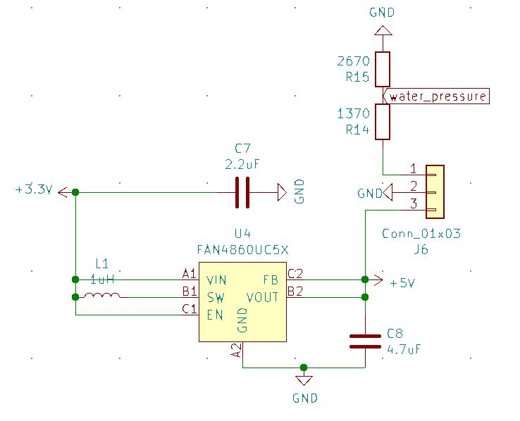
The water-pressure outside the ROV is measured using the cheapest water-proof pressure sensor I could find: “EBOWAN DC 5V G1/4 Pressure Transducer 1.2 Mpa” with the ¼ A4 of documentation available on Aliexpress it is just enough to drive it (hopefully). Unfortunately this sensor requires 5V, while all my other components are on +3V3. So I have made a 3-5V boost converter specially for this sensor (FAN3860 (U4)). Together with a voltage divider to read the analogue output of the device.
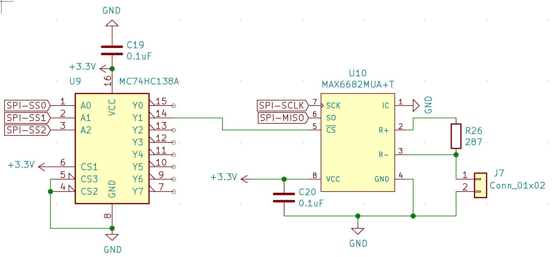
The water temperature is measured by an even undocumented sensor as the pressure sensor. The YC100665 a thermistor connected to J7. The thermistor is measured by a MAX6682 (U10) to fix self-heating and filtering for the thermistor. Communication is done with SPI and using a MC74HC (U9) for Slave-select multiplexing.
The temperature of the battery, ESC’s and possible something else in the future is being measured by DS18B20 (J9-11) sensors.
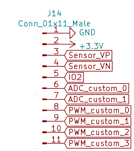
The BLHeli motors (capacity of 4) will be connected to J5. The SimonK motors are operated through an PCA9685 (U2) I²C to PWM. Four motors can be connected through J4 and another 4 with the 2.54mm pin header (J14).
The water level is measured using a ADS1015 (U3) I²C ADC. The water level sensors are connected to J15 and J8.
This is still a development board, so extra things may be connected with pin header J14. That functions as a breakdown board for unused, but useful features of the IC’s on this board.
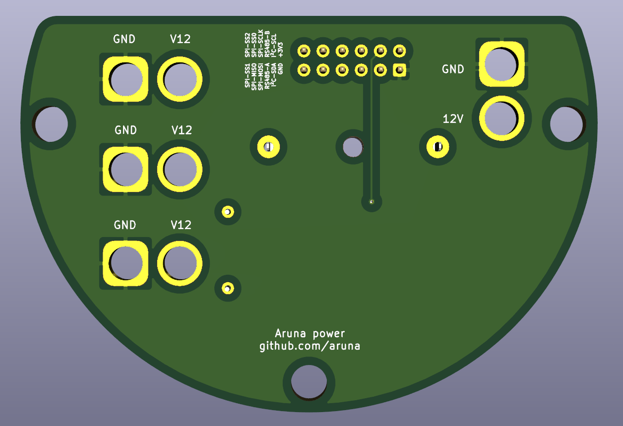
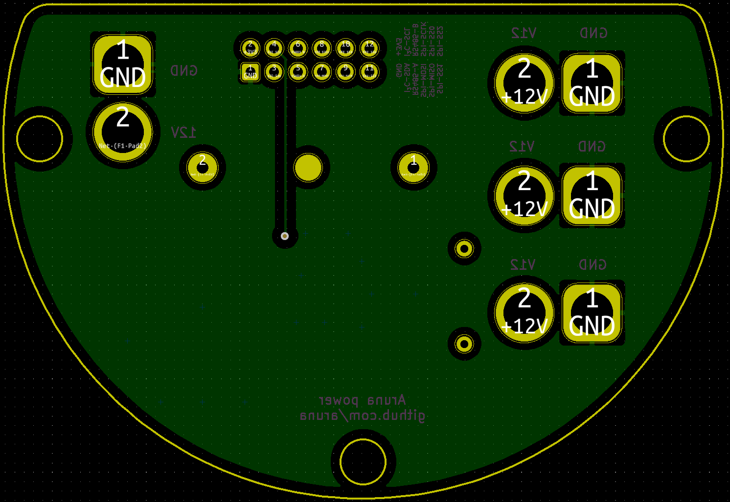
Power board
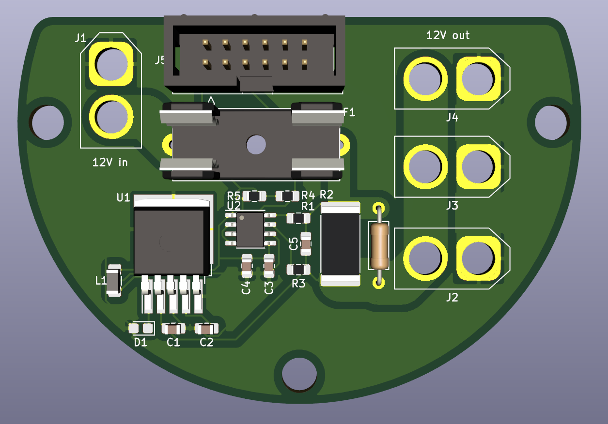
Next to the main Apsu board I also developed a board to manage the power of the ROV. This boards converts 12V into 3.3V and monitors the voltage and current levels. The power comes in though XT60 connector J1 it then follows it way though a fuse, and is fed to J2-4. A LM25955-3.3 (U1) is used to convert 12v to 3.3v. And send on the bus using J5 with the same layout as the Apsu board. The current and voltage is measured using an INA2918A (U2) this sensor communicated the result back to the main board using I²C.
Prototype board
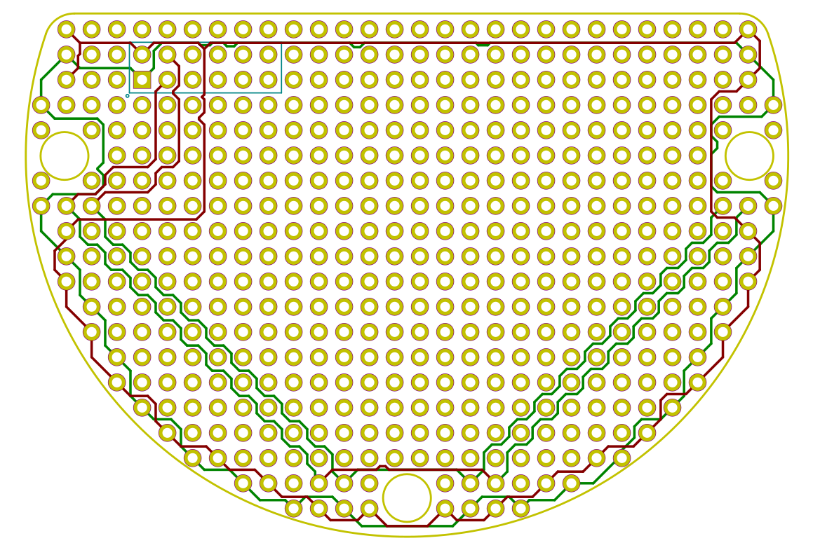
As shown in the top picture it can be quite a hazard to create prototypes in the tight space of a ROV. So for future prototyping I thought it would be nice to have a prototype boards that fits exactly in the ROV and already distributes the most commonly used pins on the bus: GND, +3V3 and I²C.
Some more images
Apsu board:
Power board
Discussions
Become a Hackaday.io Member
Create an account to leave a comment. Already have an account? Log In.