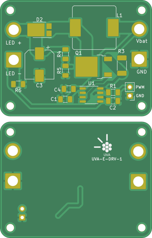
In this short log were are going to talk about some of the consideration taken into consideration when designing the PCB for the High efficiency Led Driver.

AL8853 datasheet recommendations
Thankfully, as with many integrated circuit nowadays, the AL8853 Led driver datasheet has a handful of recommendations layout. In this case they are pretty basic:
- Keep traces thick and short.
- Keep capacitors and resistors as close as possible to the IC.
- Keep delicate signals away from inductors.
- Make sure these high current loops are as short as possible.
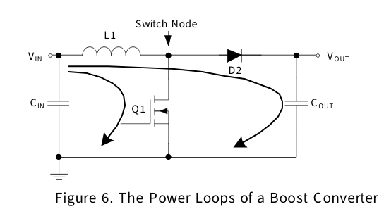
The loops they are talking about are these ones:

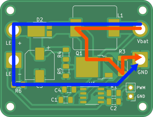
Which in our PCB, correspond to the following traces:

Which realistically speaking, are about as small as I could feasible make them.
A word about EMI transmission
I do not know much about PCB design in general. But in this excellent resource over here, they recommend the practice of via stitching to minimize the amount of electromagnetic interference your board will generate.
So if you check the Kicad project for this board and wonder why there are so many random vias everywhere. This is the reason.
 Said Alvarado Marin
Discussions
Become a Hackaday.io Member
Create an account to leave a comment. Already have an account? Log In.