 zpekic
Most CPUs contain some number of internal registers, a subset of which are available for programs to use. These are often not much more than very fast internal memory connected to internal bus(es) and ALU(s), meaning that the the transformation of bits crucial for program execution is happening elsewhere and not within logical confines of the register.
SIFP-16 somewhat extends the concept of register to a "processing element" - each of these in addition to fast value storage is also given own simple ALU, flags inputs and outputs, as well as part of control over CPU data and address paths to make it a self-contained unit of data processing.
All 5 processing elements present in SIFP-16 have the following basic internal structure:
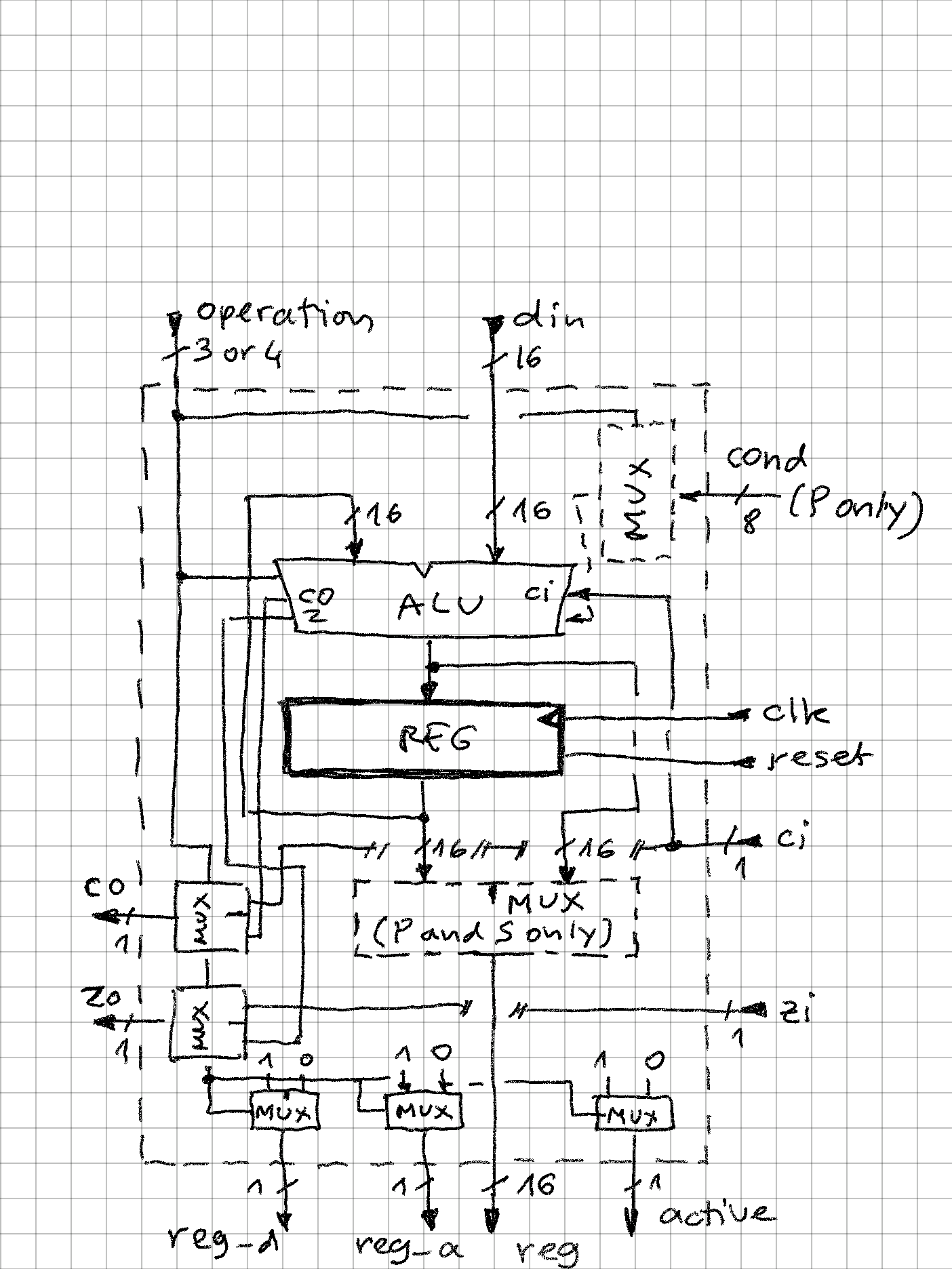
Main elements:
- 16-bit data value, "register", loaded with rising clock signal which is connected to all others PEs, and reset with also common reset signal (only for P and S is reset of importance as CPU boot depends on both being initialized to 0)
- operation - 3 or 4 control bits, selecting 1 of 7 or 1 of 15 operations (1 is always NOP). These are coming directly as a slice of the currently executing instruction code.
- single data input
- single data output
- carry and zero outputs, which depending on operation can be "passthrough" or coming from ALU
- control output signals reg_d, reg_a that drive the address and data paths
- control output signal "active" which is 0 only when operation is NOP. These signals are used to count CPU throughput, how many operations can be executed in single operation (min = 0, max = 5)
- register is updated through the ALU, which is in most cases a simple binary adder with some passthrough (e.g. NOP is always implemented as register reloading self-value)
- (optional) output MUX is needed as different value than register should be sometimes projected out (e.g. S + 1 before the value is updated)
- (optional) condition codes fed into P (program counter) branch / no branch decision logic.
Processing element operations are declared in the include file that defines the instruction field bits. This way the microcode source becomes a CPU assembly source file, and assembly instructions can use:
- any variation of the operation mnemonic (these are delimited with |)
- "aliases" which are handy shortcuts for most frequently used operation combinations (such as PUSH/POP etc.)
- each assembly instruction must be closed by ; but it can contain 1-5 operations and those must be delimited with ,
All program control depends on the operations that P supports. It is important to note that at time of execution of these operations P has been incremented and is pointing to next location in program memory, which can be used either as data (destination for jump, branch offset, immediate) or next instruction.
- STPx - because there can be no push and jump in same instruction (that would require 2 memory cycles and only 1 is possible), these allow to push "forward" P value to internal data bus
- JUMP|GOTO - allows use of absolute targets, for example system calls in ROM
- BRANCH - relative jumps can reach any target in the memory, but if confined to same module can implement relocatable code
- LDP - beside return, this operation allows jumping to location in any other processing element or memory pointed by it (e.g. LDP, X; LDP, M[Y]; etc.). This allows data driven "case" statements or dispatch tables.
// 16-bit program counter (has no flags, always increment during fetch phase, changes as below during execute phase)
r_p    .valfield 4 values
    NOP,            // continue (increment P during next fetch phase)
    M[IMM],            // output value as address, increment (used for immediate values)
    BRANCH|IF_TRUE,        // unconditional branch (add word pointed by P)
    JUMP|GOTO,        // unconditional jump (load with word pointed by P)
    LDP,            // load from incoming data (mostly from stack, for return)
    STP4,            // put P + 4 to internal data bus
    STP2,            // put P + 2 to internal data bus
    STP,            // put P to internal data bus (mostly to output during trace mode)
    BAC|IF_AC|IF_A_GE,    // if A flag C set add word pointed by P (branch), else increment P
    BAZ|IF_AZ|IF_A_EQ,    // if A flag Z set add word pointed by P (branch), else increment P
    BXC|IF_XC|IF_X_GE,
    BXZ|IF_XZ|IF_X_EQ,
    BYC|IF_YC|IF_Y_GE,
        BYZ|IF_YZ|IF_Y_EQ,
    BSC|IF_SC|IF_S_GE,
    BSZ|IF_SZ|IF_S_EQ
    default NOP;
With only 5 remaining operations (after no-op, load and store are used), the dilemma was which others to implement:
- No subtract, because it can be implemented with XOR (negate bits) and ADC
- No OR because it can be done by driving the internal data bus with more than one source (for example LDA, X, M[Y] is equivalent to A <= X OR M[Y])
- No rotate because it can be (with some inconvenience) achieved with shift
- No compare, as equality comparison can be done with XOR, and magnitute comparison with various tricks (e.g. adding the negative value of the constant)
// 16-bit accumulator (has own carry (AC) and zero (AZ) flags, changes only during execute phases)
r_a	.valfield 3 values
	NOA,	// no operation on A register
	XOR,	// logical xor with incoming data (AZ)
	SLC,	// shift left through carry	(AC, AZ)
	SRC,	// shift right through carry (AC, AZ)
	LDA,	// load with incoming data (AZ)
	ADC,	// add incoming data and carry flag (AC, AZ)
	AND,	// logical and with incoming data (AZ)
	STA|A	// output value as data
			default NOA;
X, Y (index / base pointers / counter)
These two are identical in every way. Main uses are indirect and base + index addressing, counters, temporary storage.
// 16-bit index register X (has own carry (XC) and zero (XZ) flags, changes only during execute phases)
r_x	.valfield 3 values
	NOX,	// no operation on X register
	CPX,	// compare with incoming data (XC, XZ)
	INX,	// increment by 1	(XC, XZ)
	DEX,	// decrement by 1	(XC, XZ)
	LDX,	// load with incoming data (XZ)
	ADX,	// add incoming data (XC, XZ)
	M[X],	// output value as address
	STX|X	// output value as data
				default NOX;
A very "classic" stack pointer, growing from high address towards lower. However the S points to TOS (top of stack) not the first free location on stack. So M[S] allows direct read and modification of the TOS. It is initialized at 0 after RESET, so first push will write to location 0xFFFF which is expected to be RAM (ROM is expected at 0x0000, i8080 style)
ADS and LDS allows (with some difficulty) implementation of stack frames and overflow checks.
// 16-bit stack pointer S (has own carry (SC) and zero (SZ) flags, changes only during execute phases)
r_s	.valfield 3 values
	NOS,	// no operation on S register
	CPS,	// compare with incoming data (SC, SZ)
	M[POP],	// address is S, then increment
	M[PUSH],// address is S - 1, then decrement
	LDS,	// load with incoming data (SZ)
	ADS,	// add incoming data (SC, SZ)
	M[S],	// output value as address (use to access stack top in memory)
	STS|S	// output value as data
	default NOS;
Processing elements recap:
| Processing element | Instruction bit field | Number of instructions | Flags (carry, zero) | Project data | Project address |
| P | 15..13 | 16 | (only consumes flags from A, X, Y, S) | yes (multiple) | yes (multiple) |
| A | 12..10 | 8 | ac, az | yes | no |
| X | 9..0 | 8 | xc, xz | yes | yes |
| Y | 6..4 | 8 | yc, yz | yes | yes |
| S | 3..0 | 8 | sc, sz | yes | yes (multiple) |
Discussions
Become a Hackaday.io Member
Create an account to leave a comment. Already have an account? Log In.