 NotBlackMagic
Background
The inspiration for this project came while working at home and only having a multi-meter as test equipment. The first idea was to make a simple low sample rate USB oscilloscope using the integrated analog circuits of the STM32G4, the ADC and the OpAmps with PGA. This then evolved into this DAQ project as the need for many, slower, analog input channels with differential mode became the focus. The idea is to create a DAQ with hardware feature parity with popular USB DAQs from NI, LabJack and others while having a BOM bellow the price of those options. Of course the software compatibility and features will be way more limiting.
Hardware
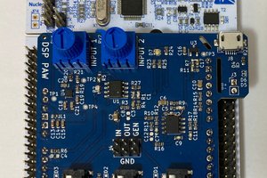
The heart of the DAQ is the new STM32G4 MCU which is used for control, USB Interface and for its ADCs and DACs. The board is designed to also use dedicated external ADC and DAC for increased performance but higher cost.
For the analog input signal conditioning the ADA4254 is used in combination with the DG409 Multiplexer, to get the desired number of analog input channels. A trade of between sample rate and circuit complexity was made by splitting the analog input into two identical blocks with each it's own ADC and input signal conditioning. Each of these blocks has 4 differential, 8 single ended, input channels, one programmable current source and two analog outputs, besides 5V and 3.3V outputs. The analog outputs are simply amplified outputs of the MCU DACs, two DACs per block.
The positive and negative voltage rails needed are derived from the USB supply using a combined Boost and Inverter switching converter, the TPS65130, in combination with a combined positive and negative rail LDO, the TPS7A39, for noise reduction.
The DAQ also features a digital interface with 16 channels/pins, each working with 5V signals due to integrated level shift circuitry. All these pins are located on a DB-25 connector.
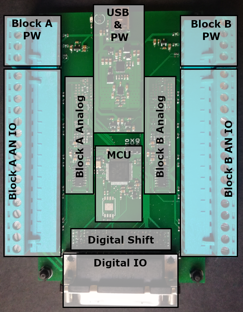
The figure bellow shows the arrangement of the different circuits and connectors on the PCB.
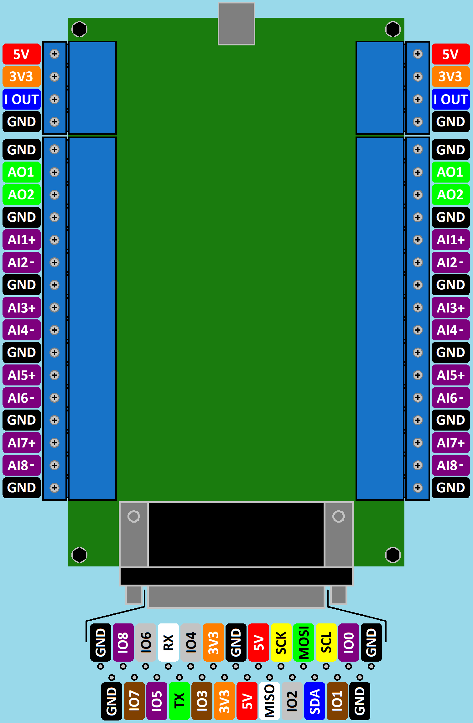
The pinout of all the connectors is shown in the figure bellow:
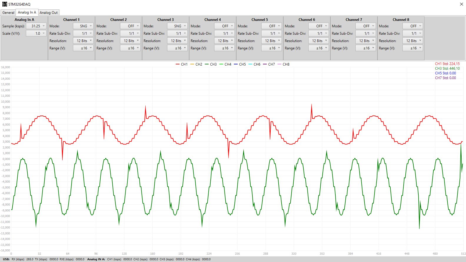
Results
The analog input is limited to 62.5 ksps shared between all channels of an analog block. This is manly due to channel switching speed, the ADA4254 has to be reprogrammed after each acquisition to switch gain settings, the external multiplexer (controlled by the ADA4254) and the input mode. Also to note that for the best performance, lowest noise and offset, the sampling frequency has to be a even integer division of 125 kHz because the ADA4254 is a chopping amplifier with a chopping frequency of 125 kHz.
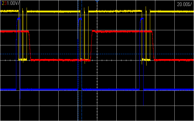
The timing of the analog input can be seen in the figure below, in yellow is the CS line to the ADA4254, in blue is the ADC ISR timing, goes high when an ADC conversion is complete, and in red the output of the ADA4254 when sampling two channels, one at -0.9V and the other at 0.9V.
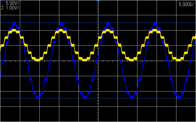
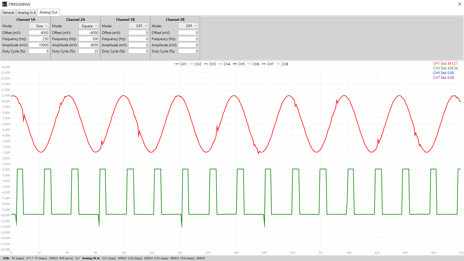
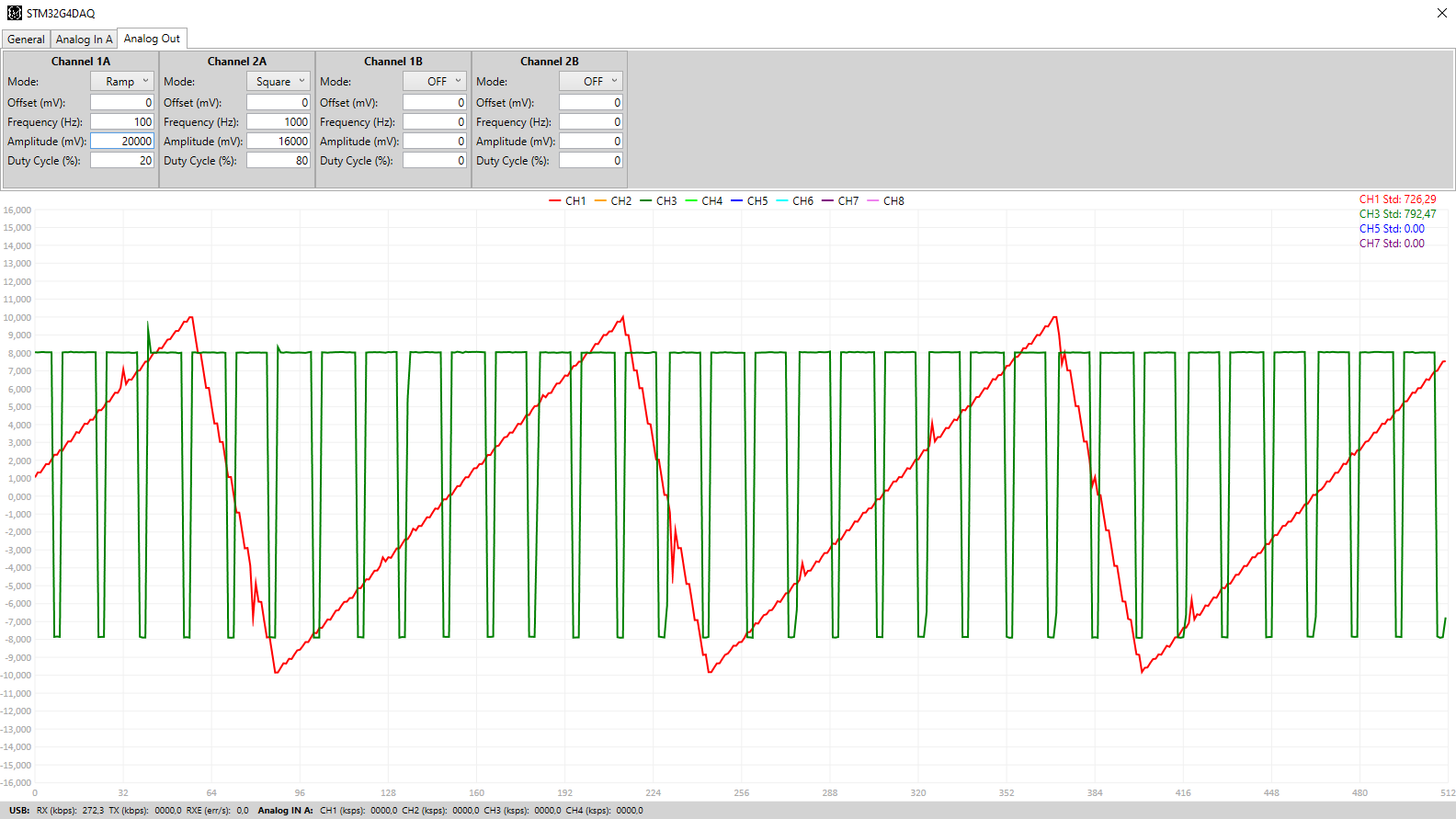
The analog output is limited to about 250 ksps when using full scale steps, -12V to 12V. This limitation comes from the low slew rate value, 9 V/us, of the amplifier currently used. To achieve the maximum sample rate of 1 MSPS, limited by the STM32G4 DACs, an amplifier with a slew rate of over 24 V/us is needed.
This amplifier will be exchanged in the future even though this limitation is not very important as to get any other signal besides a square wave more then one sample, multiple steps, are needed which decreases the necessary slew rate. This is shown in the figure bellow where a full scale sine wave is generated using 12 samples/steps @ 1 MSPS without a problem. In yellow is the DAC output and in blue the analog output after the amplifier.
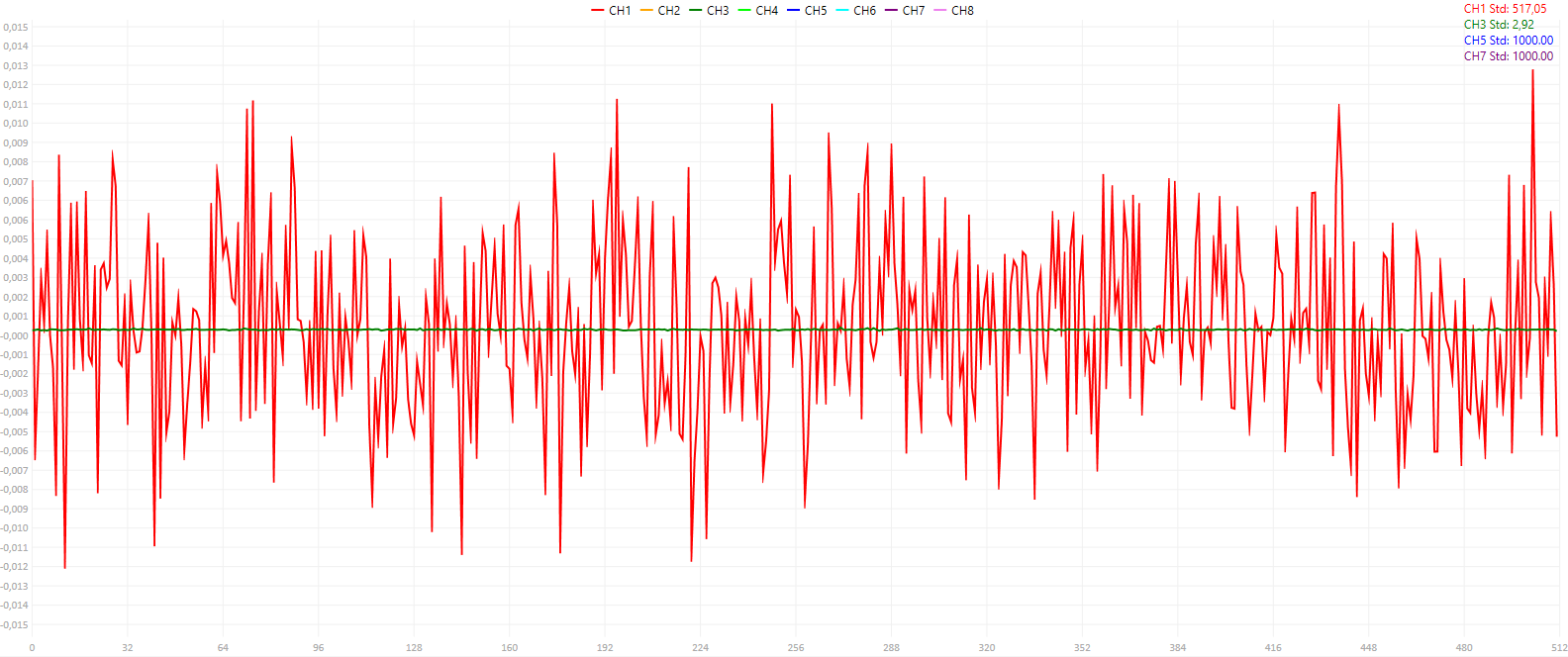
The Digital IO, with the current level shift circuitry, is limited to signals bellow 1 MHz and has an input and output impedance of 1 kOhms. Both of these limitations are due to the level shift circuitry used, a simple single MOSFET level shift circuit, and is mainly dictated by the pull-up resistor value. This can be seen in the figure bellow where a pull-up...
Read more »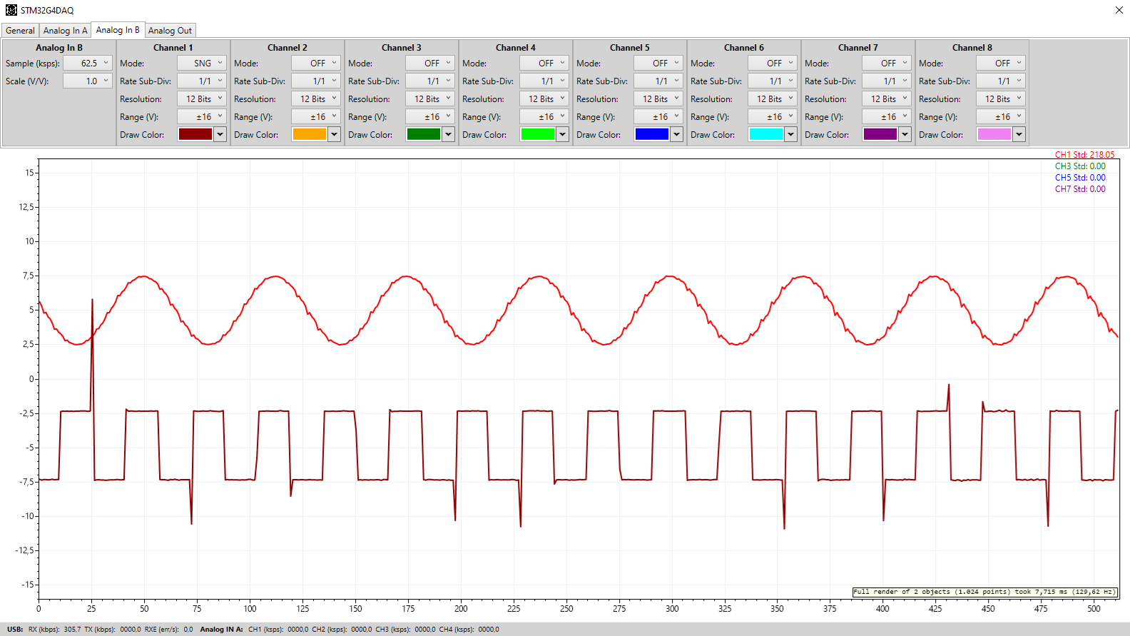

 Clyne
Clyne
 doctek
 Marc René Schädler
Nice project!
I am looking for a low speed industrial IO isolated analog ouput board for 0-10V hence my interest in this project.
Note that you need another analog output opamp as the TLV9002 from the schematic has an absolute maximum supply voltage differential of 6V supplied by +14V /-14V, I read that the tests were done with an OPA1678, maybe update the schematic?