 Tim
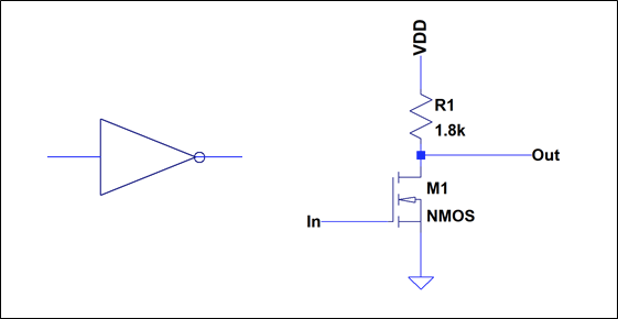
TimThe most basic NMOS gate, an inverter, consists of a load resistor and an N-MOSFET as shown below. NAND and NOR gates can easily be formed by using two N-MOSFETS, more complicated gates are formed by combinations thereof.
Some benefits compared to Resistor-Transistor-Logic are:
- Lower component count since no base resistor is required
- Since no current flows into the gate, the fan-out behavior is much more forgiving. It is not necessary to scale the load resistor according to the number of gate connected.
- Stacking of transistors to form NAND gates is easily possible. In contrast to RTL, no issues with load instability or parasitic current paths are observed.
- The logic levels are well defined by the threshold voltage of the NMOS.
In short, it is much easier to realize discrete logic circuits without spending a lot of thought on analog circuit design.
The Catch
There is a drawback, isn't there? Two things stand out:
- The MOSFET is a four terminal device. To build fany circuits like pass-transistor logic or cross coupled XOR gates we also need to to control the substrate contact.
- Somehow it seems that all practical examples of discrete NMOS circuits are very very slow, as evidenced by the Megaprocessor and the Monster6502. Let's figure out what to do about this.
Types of discrete MOSFETS
Although often no distinction is made by the circuit symbol, there are actually several different types of MOSFETS.
Planar MOSFET
The basic type of MOSFET that is also used in integrated circuits (at least up to the 32 nm node) is called the planar MOSFET. A cross section is shown below.
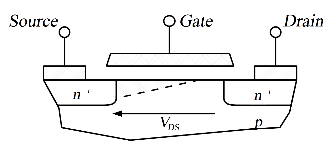
Both source and drain contact are accessible from the top of the device, while bulk contact can be established by contacting the subtrate by a p+ region at the bottom or next to the S/D junction.
Power MOSFET
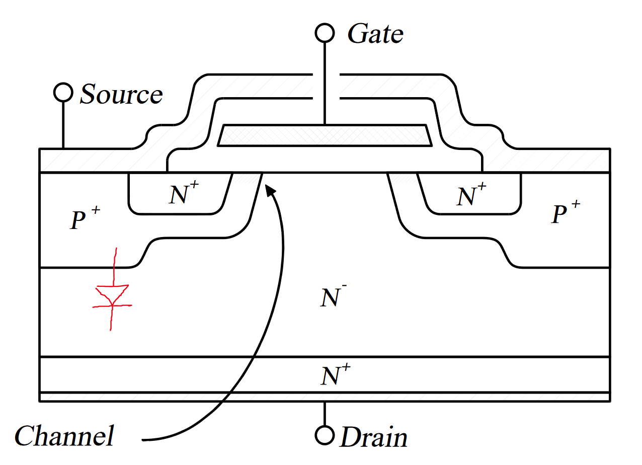
DIscrete MOSFET are often used as switch for high currents. These applications are typically addressed by a functionallity similar, but differently constructed device called the Power-MOSFET. A cross-section of the basic structure is shown below. Note that there are many variants and refinements of this devices. Each power-MOS consists of many of the cells as shown below.
 CC BY-SA 3.0, https://commons.wikimedia.org/w/index.php?curid=538889
Compared to the planar device, the current flow through the power-MOS is vertical. The source is at the top and the drain is at the bottom. The bulk is directly connected to the source. Due to this, it is not possible to control the bulk contact independently anymore and a PN-Diode is formed between source and drain. This is given by design and is not a disdavantage for most application. It does, however, prevent us from using these devices in a pass gate configuration.
Discussions
Become a Hackaday.io Member
Create an account to leave a comment. Already have an account? Log In.
"It does, however, prevent us from using these devices in a pass gate configuration."
Unless you connect 2 such devices with their diodes back-to-back.
It's more expensive but "it works" well enough in some cases.
Are you sure? yes | no
Yes, but you also double input capacitance, channel resistivity and footprint :) Maybe that is ok in some use cases though, like flipflops.
Are you sure? yes | no