 Tim
TimNow that we settled on having to use power mosfets to build our NMOS gates, the question still remains which of the transistors that are available is best to use.
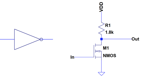
The basic NMOS gate is an inverter, as shown above. As a rough guideline, we would like to optimize the following criteria:
- Acceptable Power consumption
- High speed
- High noise margin (Voltage difference between switching levels and logic levels)
The practical implementations of these requirements can be easily explained by the NMOS inverter circuit.
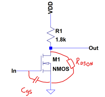
Given the simplified inverter circuit above, we can derive the relevant parameters like this:
| VoutH = VDD | Output high voltage [V] |
| VoutL = VDD * RDSON / (R1 + RDSON) VoutL ~ VDD* RDSON / R1 | Output low voltage [V] |
| VLH = VHL = Vth | Input switching threshold [V] |
| VMargin = Vth - VoutL ~ Vth - Vdd* RDSON/R1 | Logic Level noise margin [V] |
| Istatic = VDD / (R1 + RDSON) ~ VDD / R1 | Static load current [A] |
| tpdLH ~ Cgs * R1 tpdHL ~ Cgs * RDSON | Propagation delay [s] |
Firstly, it is obvious that there is a speed/power tradeoff when chosing the load resistors R1. I picked 1.8 kOhm since I used this before. This leads to a static consumption of about 3 mA, which is only acceptable for small designs (or when you build a 60ies style supercomputer).
Typical values for Vth are 1-2 V. Therefore we want out output low level to be significantly below this. For VDD=5V, it follows that 10 * RDSON < R1. Hence RDSON should be lower than 180 Ohm, which is quite high.
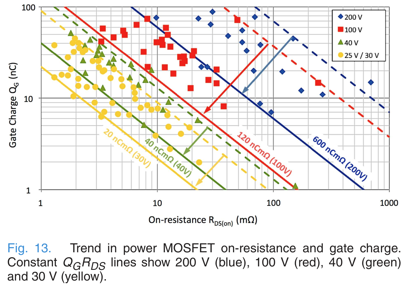
Finally, to optimize speed, we would pick a transitor with a Cgs as small as possible. Since the gate capacitance of a DMOS transistor is highly dependent on gate voltage it is not possible to assign fixed large signal capacitance. Instead typical the cumulative charge needed to turn on the transistor is quoted as gate charge Qg.
To summarize, we need a power mosfet with the following properties:
- RDSon < 100 Ohm
- Qg as small as possible
- VDSMax >5V
- Vth 1-2 V
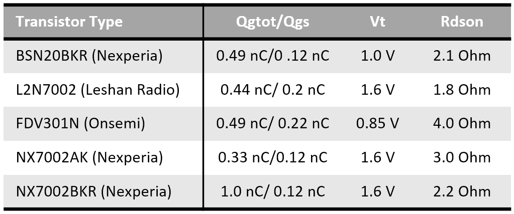
A list of candidate devices is shown below. Most of these are variants of the ancient 2N7002. The FDV301N is a device targeted at replacing digital bipolar transistors and therefore appears to be especially suitable.
Discussions
Become a Hackaday.io Member
Create an account to leave a comment. Already have an account? Log In.