I often need a DC-DC bias supply for my projects that supplies a few outputs, typically 5V & 12V, only a few watts, and most often non-isolated. There are a lot of COTS choices in this range with unit costs under $20.00 but I often find that they don't meet some key spec. Most often it is the dual output requirement combined with a Vin range from ~10V ~ 25V. In the past I've worked around this by going with a single 12V output followed by a 5V linear regulator. Not a big deal but it is more parts to source & place along with a bit more dissipation.
I've often kicked around the idea of designing one that has some configuration flexibility but I didn't want to spend the time (a 5W design can demand as much time as a 500W). Once more I find myself needing one for my Solar Charger and this time the itch got the better of me.
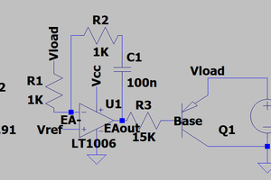
I had one of TI's LM5017 evaluation boards lying around and decided to give it a go. The attraction to the LM50xx family of regulators is their simplicity, small parts count, low cost, wide V_in range, and output configuration flexibility. They are non-isolated buck regulators but you can add additional windings to obtain additional outputs at different voltages. Those outputs can be isolated or tied to the primary ground. A constant on-time PWM scheme is used which eliminates the traditional compensation network required to close the control loop.
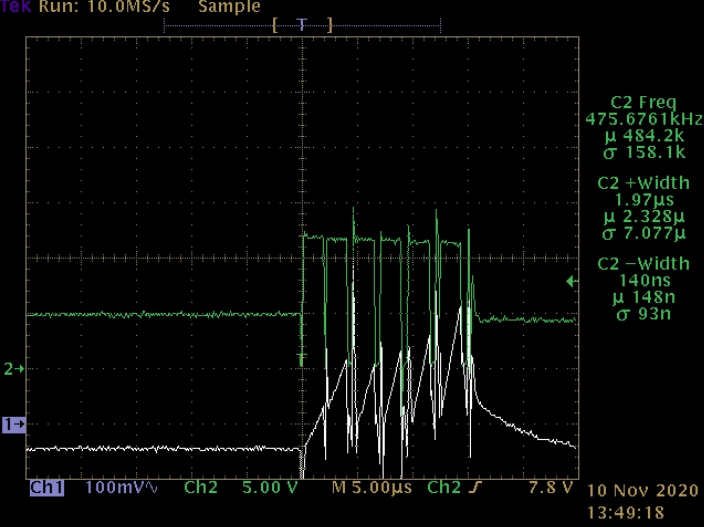
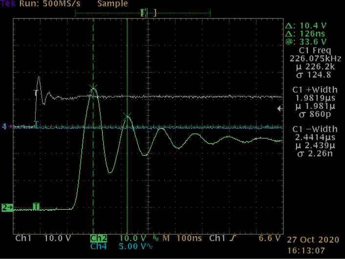
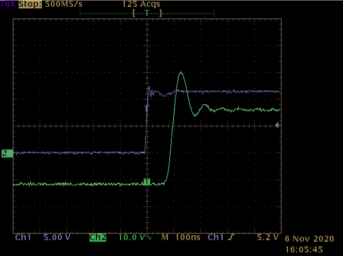
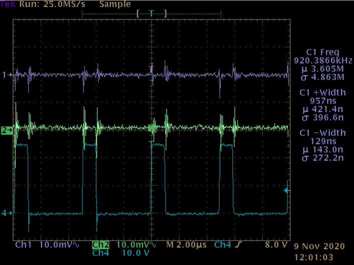
A quick characterization of the LM5017 showed that output ripple was a problem.
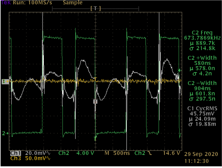
This is an artifact of the constant on-time control scheme: the control loop requires ripple for stability (a contributing factor is the small output capacitance).
Adding an small LC filter to the output solved this problem.
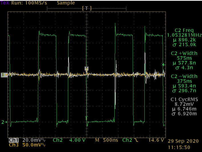
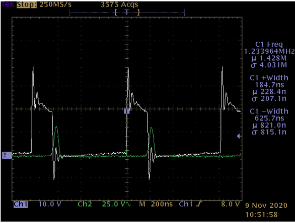
The LM5017's other problem is its current limit of 600mA which wouldn't be enough to handle power required of both outputs. No problem, the LM5161 is its higher power sibling that also integrates a few other features that the LM5017 requires discrete components for.
So, down the bunny hole I went.
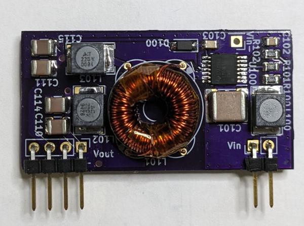
The design was done in Kicad and the project is posted. It includes improvements from the article in the pictures. Also posted is my design workbook based on TI's datasheet guidance. Note that the as-built uses all MLCCs vs. electrolytics for output capacitance: this was done for space & cost and does not materially effect performance.
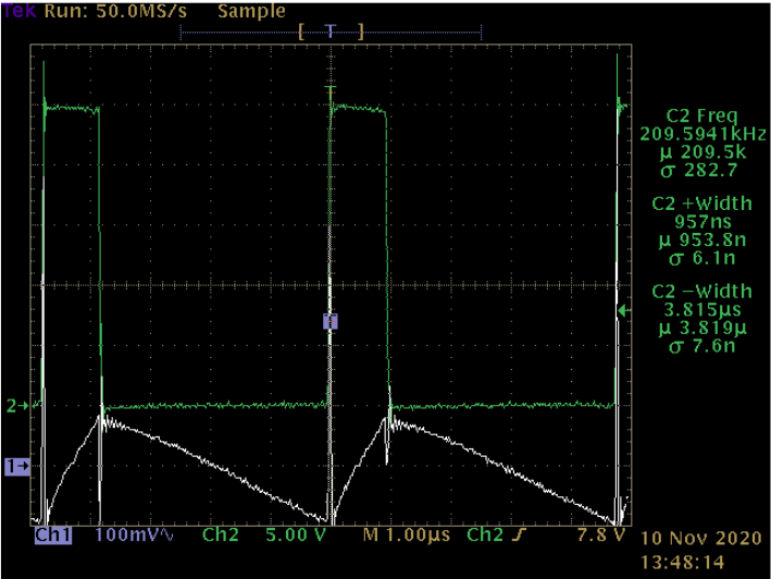
The logs provide additional detail on the design, build, and limitations: be sure to read them before you decide to build it. The design, inherent to the controller architecture, has problems:
+ Conditional stability
+ Secondary regulation
+ Current limit scheme
As long as these are understood it can be used successfully. I will likely use it in the prototype of my Solar Charger for a real-world test.


 Evangelos Petrongonas
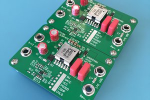
 James Wilson