 Ken Yap
Background
I have National Semiconductor MM5371 chips from the 70s. I made a clock using it back in the late 70s which I restored in this short project. However the board leaves a lot to be desired due to my inexperience at the time. Since I have 5 chips, I decided to design a proper circuit and PCB for it which will mate with my previous projects, large 7 segment or 6 segment cascadable displays. With today's high efficiency LEDs the display can be very bright.
I admit to nostalgia for this chip, as it was one of my first major projects back then.
The objectives of this project are to build a mains frequency based clock with a large, bright display, and to explore circuit ideas.
Specifications
Chips of this era were PMOS technology, so voltages are relatively high, in this case from 21-29V although it will function down to 8V. The large voltage swing gives a lot of noise immunity and ability to operate over a wide range of voltages, no regulated supply required, good for consumer devices. The high integration makes up for the semiconductor limitations.
The chips are slow by current standards; the maximum supported switching rate is 60kHz, but time of day clocks don't need high frequency capability. The timebase is the mains supply; the MM5371 is a 50Hz based clock. This means I have to use old school transformer power supplies as modern switching mode power supplies don't supply a mains frequency. On the other hand the long term accuracy of the mains is very good.
Other features made it easy for clock designers. Aside from the display circuit, it only needs an RC mains frequency filter, a RC circuit for the multiplexing oscillator, and buttons. The control pins have depletion load pulldowns so external pulldown resistors are not needed.
I'm taking advantage of the high supply voltage for driving chains of LEDs. For example LEDs with 3V forward voltage will require 12V for a chain of 4, more than a standard 5V supply.
The datasheet is supplied in the files section.
Design
The first design choice is whether to base the common ground on Vss or Vdd. This was easy. The open drain PMOS transistors are relatively weak and so the on voltage is several volts below Vss. So the common ground will be Vdd. The main exception is the settings buttons which are referenced to Vss. A little mind twisting is required to read the datasheet which uses Vss as the reference. We will drive the chip and the LED chains from a nominal 24V, and 5V from a regulator will be used for the interface logic.
The digit drivers are NPN transistors which will turn on when the digit is active. This will drive the PNP transistors on the LED PCB.
The segment driver logic is reversed; they turn off to light the segment because it was designed to drive plasma displays using capacitive coupling. You can see from the datasheet that the open drain PMOS transistors can hold off 45V.
So an inverting stage is needed for the segment drivers. Instead of transistors I have chosen to use level shifters and a 2764 EPROM as the translator chip, and open collector 7406 or 7407 TTL chips as segment drivers. At the time this clock chip came out and for years afterwards, this would be an unthinkable choice as these chips would have cost far more than the clock chip and a horrendous waste of EPROM space. Discrete transistors and passives would have been used. But I am no longer constrained by the past, and I have heaps of these chips in my junkspares box so I can indulge in an unconventional design. It allows me to adapt to 7 segment or 6 segment digits with a change to the EPROM contents. It reduces PCB space and soldering compared to a more discrete design.
Analysis shows that 5 segments suffice to uniquely identify the digit being displayed so the EPROM serves as a 5 input to 6 or 7 output map. The Python program that generates the map is in the files section.
Circuit
I went through a couple of iterations of the design on "paper" working on and off...
Read more »
 Charles Ahrens
 Litan Virgil
 SwiftyTheFox001
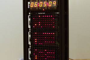
 Ted Yapo