 Jeremy Ruhland
There are a variety of inexpensive (<$100) entry level near-field probes available from the usual suspects, however I've been dissuaded from purchasing them for the following reasons:
- Fly by night operations: How long will this random ebay item be available? Will there be any other source for this model of probe? Where did this come from anyway? The seller certainly has no association with the designer.
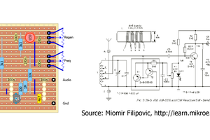
- Documentation: Most of these things lack a named manufacturer and model number. What kind of response and characteristics was it designed to have? At best you get a grainy jpg showing a possibly fake frequency response curve with unlabeled axis. How is it different from other similar models from a hundred other nameless ebay vendors?
- Design: Were these things actually...designed? All the cheap probes are fabricated on 2 layer PCB stackups and lack adequate electrical shielding. Some of these traces look like they /might/ be 50ohm but others definitely aren't. Without documentation there's no way to verify the intent of the designer. Maybe some of these probes are okay but none of them show it and I would have to buy them all to check.
I aim to solve some of these problems with Open Field Probe. Minimal effort is required to improve the basic designs. At the very least you will be able to download CAD files and gerbers and know where they came from.
 agp.cooper
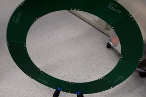
 Denys Zaikin
 mircemk
 Andrew Ferguson
Oh my god. I was considering designing something likes this for our company. I will definitely show this to my boss, since its pretty hard to convince management we need a set of well documented field probes.