Close
0%
0%

STEbus 6845/6803 video board

Reverse engineering a colour graphics video board

Similar projects worth following
An STEbus video board sounds a nice project, as it demonstrates mastery of video signal generation. Showing video on domestic tellies avoided the need to buy expensive terminals and thus kick-started the home computer revolution.
There is not so much call for it these days. Domestic tellies have HDMI inputs, requiring GHz signal rates which are beyond simple home-made prototyping.
However, this page looks at some designs that might be good starting points.

I expected this to be extinct, but Steve told me he had one AND the manuals for the hardware and software! He kindly scanned them for me and very kindly posted the board to me! It is serial number 2 - the second one ever sold!

The software manual includes a listing of the start of the ROM, which shows the names of many variables, jump tables, and the names of functions being jumped to. This is a great help. I have assimilated this into the regenerated source code. The labels have had the '.' character replaced with "_" because my assembler rejected the former.

J031-U5.eqn.txt

STEbus interface. Analysed but not verified.

plain - 2.14 kB - 11/05/2022 at 01:55

Download

J031-U5.EQN

Disassembled JEDEC file.

eqn - 1.26 kB - 11/05/2022 at 01:55

Download

J031-U7.eqn.txt

Decodes the MPU memory map. Analysed but not verified.

plain - 1.71 kB - 11/05/2022 at 01:55

Download

J031-U7.EQN

Disassembled JEDEC file.

eqn - 859.00 bytes - 11/05/2022 at 01:55

Download

J031-U32.eqn.txt

Video timing generator. Analysed but not verified.

plain - 1.51 kB - 11/05/2022 at 01:55

Download

View all 20 files

  • The SGT1 address multiplexer analysis​

    Keith11/02/2022 at 23:26 0 comments

    The 4-to-1 bit multiplexers select input bits based on signals B and A.

    "B" is VCYC inverted.

    "A", the Row/Column selector, is /RAS clocked by the 28 MHz master clock.
    This is /RAS delayed by 1/28th of a microsecond, which is 35 ns.

    /CAS is /RAS clocked by CY3, which is half the 28 MHz master clock.
    This is /RAS delayed by 1/14th of a microsecond which is 71 ns.

    DRAM cycle frequency is 28/8 = 3.5 MHz.

    inout
    video (VCYC=1)mpu (VCYC=0)
    rowcolrowcol
    ra0ma5a0a8xa0
    ra1ma6a1a9xa1
    ra2ma7a2a10xa2
    ma0ma8a3a11xa3
    ma1ma9a4a12xa4
    ma2ma10a5a13xa5
    ma3ma11a6a14xa6
    ma4ma12a7a15xa7

  • The SGT1 ​state machine analysis

    Keith11/02/2022 at 00:25 0 comments

    This is the primary timing generator.

    Rather than trying to capture screenshots of my logic analyser, it is easier and quicker to write a small C program to simulate it. So I did. See file J031-U27-analyser.c.

    The waveforms look like this (state at the bottom, data above, white shaded is one MPU cycle):

    from which we can deduce:

    • The MPU cycles every 24 clock ticks. 
    • For a 28 MHz clock, the MPU cycles at 28/24 = 7/6 = 1.166 MHz.
    • That gives exactly 224 MPU cycles per 64 microsecond line.
    • And 160 MPU cycles of display time are 45.714... microseconds.
    • MPU clock duty cycle is 11 high to 13 low.
    • There are four /RAS cycles, each six clock ticks long.
    • Three happen when VCYC is high (video access)
    • One happens when VCYC is low (MPU access)
    • States 1, 3, 5, 7, 10, 18, 20,25 are illegal, and sweep to state 0.

    The DMS72S288 pinout is:

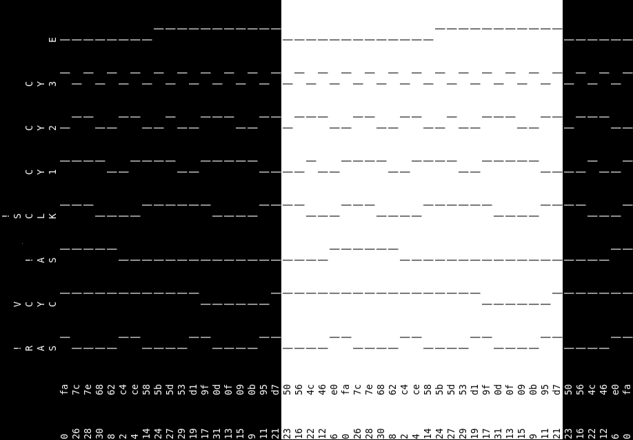
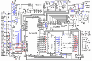
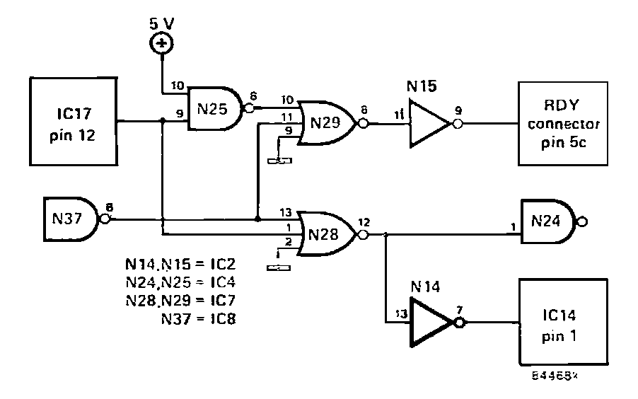
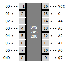
    I had a long hard look at the binary sequencing, the see if it could be implemented in a 16V8 GAL.
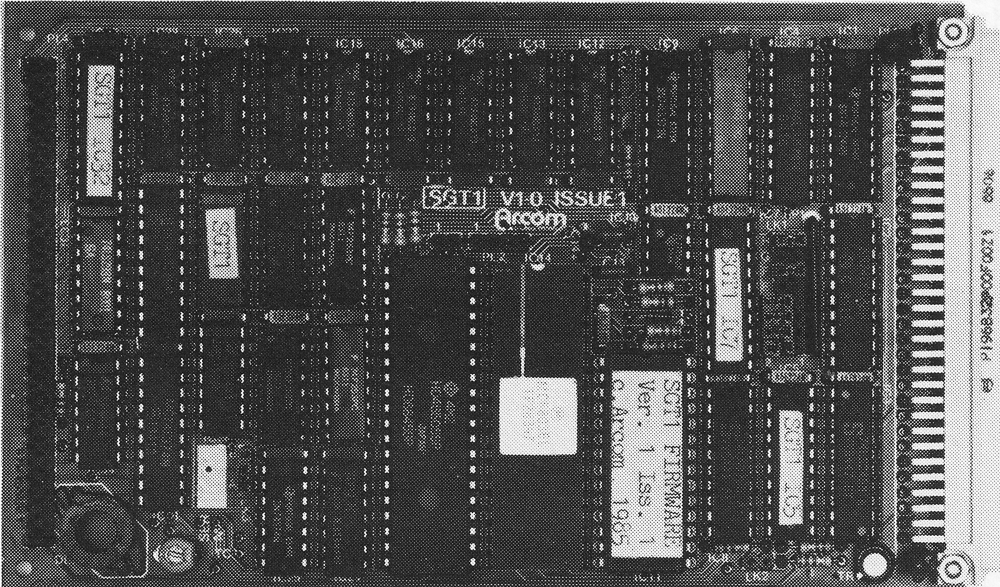
    CYC3 is easy, inverting every clock cycle.

    The rest do not have an obvious pattern. The PROM allows any random sequence. A GAL would have to decode 32 OR terms to do the same. I expect the designers wanted to keep the flexibility to cope with potential changes. I think I'll leave this part of the circuit for now. 

  • The Acorn 80x25 Video board

    Keith03/27/2022 at 21:28 0 comments

    2022-03-27

    Someone made replicas of some Acorn System boards, including the VDU. He also made an enhanced version. I bought one of the latter from eBay.

    It is 80 × 25 text, holding a single screen in 2k bytes of RAM. It uses four 2114 RAM chips. I would have preferred a single 6116 or 6284 chip, as these are more common.

    The characters are 6 pixels wide, which helps pixels stay clearer in the limited bandwidth monitors. The character rate is 2 MHz and the pixel rate is 12 MHz. There is a circuit to multiply the 2 MHz processor clock by six, though it is not as good as dividing 12 MHz down to drive the CPU clock. 

    The characters are 10 lines high, giving 250 lines total.

    I bought this board as an experimental platform. It saves me a lot of wiring.

    I have a strong preference for square pixels. The correct pixel rate is 14.75 MHz for 80 × 8 = 640 pixels in 43.39 microseconds PAL display time. For 80 × 6 = 480 pixels in the same time, pixels are no longer square but the pixel rate is 14.75 × 3/4 = 11.0625 MHz. The nearest commonly available frequency is the 11.0592 MHz baud-rate frequency.

    High-bandwidth video CRT monitors have become very rare, but old televisions with baseband video input are still available on eBay. I shall be modifying this board to work with the old Toshiba colour TV that I have. I intend to go with 40 columns, 8x10 character cells, and a 7.375 MHz pixel rate.

    The 6845 can be programmed for a wide range of video timings, so that should not be difficult.

    There is even an online calculator to do the work for you: https://mrboot.de/mc6845.php

    2022-04-15

    Wanting to get it up and running quickly to check it all works before making modifications, I shopped around for 2114 chips. The best deal seemed to be ten for £14.33. Searching for four-bit SRAM, I found some that are larger (16k × 4) and much larger (64k × 4). I bought some of the latter at £3.94 for four. They are 24 pins instead of 18, they have most of their pins in common. This will make them easier to shoehorn in than a RAM chip with and 8-bit data bus. As well as being cheaper, I get 64 times more memory, enough to support pixel graphics.

    Much of the minor parts and 74 series discrete logic seems to be for multiplying the 1 or 2 MHz CPU clock signal into a 6 MHz dot clock. I intend to avoid this ugly kludge by dividing a dot clock to produce the character clock.

    Shopping around for discrete logic chips is a chore. Suppliers like Mouser and Digikey have minimum order values, and chips from eBay tend to be much more expensive in ones and twos. Often several pounds instead of a several tens of pennies. 

    I'm not keen on keeping loads of 74 series logic chips around, so I shall use GAL chips for my experiments. 

  • Catalogue page

    Keith12/15/2021 at 00:58 0 comments

    STEbus Colour Graphics and Text

    SGT1

    The SGT1 brings high-resolution colour graphics to the STEbus. Graphics and text can be mixed on the screen, and the on-board 6803 processor with 64 kbytes of RAM and a 6845 CRTC deals with graphics generation and terminal emulation.

    High-level graphics commands are implemented in the 8 kbytes of on-board firmware, so the user can easily generate text, lines and arcs by I/O commands on the STEbus. Other commands can change resolution and download memory, programs, character sets and terminal commands.

    Basic resolution is 288 lines by 640 (4 colours) or 320 (8 colours). Text modes are 32 lines of 20, 40 or 80 characters.

    Outputs from the SGT1 are RGB.

    The SGT1 can be extended with an SGTX extension board which provides genlock to external video sources.

    Interface: STEbus slave.

    Power consumption: Typ 1.2 A @5V

    Features:

    • High-resolution colour graphics and text
    • 320 × 288 pixels (8 colours)
    • 640 × 288 pixels (4 colours)
    • On-board firmware
    • Simple but powerful graphics commands

  • The Retrobrew VDU board

    Keith02/12/2021 at 18:45 0 comments

    Another 80-column text-only board.

    https://retrobrewcomputers.org/doku.php?id=boards:ecb:vdu:start

    I heard of an ECB-to-STE bus interface, though this is not published on the web.
    If it exists, it would be a handy way of prototyping STEbus versions of ECB boards.

    I'm not keen on this design, because there is no direct access to a memory mapped screen. You can tell because there are no video memory address multiplexers. While this might be fine as a teletype terminal, it might be rather slow for things like games.

  • The Elektor Junior VDU board

    Keith02/12/2021 at 17:58 0 comments

    This had 2K of RAM for an 80-column display clocked at 15 MHz.

    The ideal clock rate for PAL TV is 14.75 MHz, but 15 MHz is still better than the 16 MHz of the BBC micro.

    The hardware and software are well documented.

    Werner Beukes recreated this, and the other Junior Computer boards, in modern CAD, and you can download and recreate the boards using the Gerber files from here:

    http://retro.hansotten.nl/6502-sbc/elektuur-junior/build-a-junior/junior-gerbers-by-werner-beukes/

    The board was not 'noise free', but a noise killer circuit for a 65C02-based Junior board was published in 1984. This made the CPU wait briefly if required.

    IC17 pin 12 is the Display Enable signal (DEN) from the 6845.

    IC8 pin 8 (N37) is the address decoder output, active low for the 2K video memory space.

    When the display is enabled and the CPU tries to access the video RAM, it will be told to wait (RDY goes false).

    N28 now ensures that the 6845 always has access to video RAM when display is enabled, and the CPU has access at all other times.

    I note that DEN is high for about 40 microseconds per line. This is a fairly long time, unlike the fine-grained Phi-2 interleaving on the BBC micro. A more sophisticated circuit might try to interleave access. 


    Elektor july/august 1984

    Screen-noise killer for the VDU card with the CMOS Junior

    The VDU card published in Elektor number 101, September 1983, sometimes lets noise appear on the screen, such as when a program is being listed.  This fault can easily be remedied by means of a few gates in the VDU card that are unused in the Junior Computer/VDU card combination.

    The trick of the circuit consists of stopping the processor when it attempts to write to the video RAM during the display enable time. 
    Only the 65C02 can be stopped during writing so this circuit operates exclusively with Junior Computers equipped with the CMOS Processor. 
    This procedure causes a slight delay in the output of a program but this is hardly noticeable in practice.
    In order to carry out the modification the following IC pins on the VDU card are bent out to the side so that they are no longer in the IC sockets:

    IC2 pins 7, 9, 11 and 13
    IC4 pins 1, 8, 9 and 10
    IC7 pins 1, 8, 9, 10, 11, 12, and 13 
    IC8 pin 8
    IC17 pin 1.

    These pins are then connected together as indicated by the heavy lines in the circuit diagram. 
    Pin 1 of IC17 simply remains open, while pin 2 of IC7 is already connected to ground. 

    Note that pin 1 of IC14 and pin 12 of IC17 must remain pushed into their respective sockets even after wires are soldered onto them.

    Another possible 'extra' for the VDU card is to show a frame on the monitor within which all the video data is displayed. All this requires is a single 1k resistor connected between pin 5 of IC17 and the collector of T1.

  • The SGT1

    Keith02/12/2021 at 17:55 0 comments

    The SGT1 was an STEbus colour graphics video board based on the 6845 with a 6803 microcontroller and 64K of DRAM. The 6803 drew text characters on the pixel graphics display. 

    It was quickly superseded by more advanced video boards, and the hardware details are lost. I can't recall much about it, apart from that it ran quite warm and was expensive - around twice the cost of a processor board.

    The catalogue page says there are up to 640 × 288 pixels in 4 colours. 

    640 pixels, 2 bits each = 1280 bits = 160 bytes. 320 pixels, 4 bits each = 1280 bits = 160 bytes.

    So it looks like it is reading 160 bytes per line, with 224 bytes per 64 microsecond scan line, the character clock must be 3.5 MHz and the dot clock is 14 or 7 MHz. 

    I did not think the 6845 could run that fast, the BBC Micro had a 68B45 running at 2 MHz character rate and 16 MHz dot clock. The HD46505 data sheet says it can run at up to 3 MHz. Perhaps the designers took the liberty of overclocking it? Truly square pixels would need 14.75 MHz dot clock, and 3.6875 character clock, so maybe the designers didn't feel able to overclock it that much.

    Disassembling the firmware might reveal hardware details. First thing I looked for were 6845 initialisation values.

    Looks like it is at F0B6, the first two values of 224 and 160 concur with expectations. I think the first should be one less, i.e. 223, but many 6845 firmware examples seem to forget this. It makes 0.45% difference, hence seldom noticed.

    Now that we know this is the table of initial CRTC values, we can see where they are being sent, which will show the CRTC address. E178 is the loading routine, 0400 seems to be the CRTC address.

    2022-10-21

    Hardware and software manuals arrive, allowing me to confirm many details and add many others.

    From the hardware manual, I see the video timing is from an LC delay line oscillator, running at a strange frequency of 26.75 MHz. This is almost the 27 MHz often used in video circuits. I don't know why they chose this frequency. Maybe it is a typo and they meant the 27.75 MHz that is used in teletext timing.

    I applied power and tried measuring the frequency, but my meter did not give any plausible readings. It is rated to 60 MHz but I doubt it can do so with ordinary probe leads. Coaxial cable would be better.

    I measured the character clock of the CRTC as 3.535 MHz, which is 1% above the 3.5 MHz expected in a 28 MHz system. I shall assume that 28 MHz is the designer's intent, and that the manual is wrong.

    The HD46505 is rated to CLK = 3 MHz, the original 6845 is rated to 2.5 MHz. So the HD46505 is being overclocked.

    The MC6803EL seems to be clocked at a third of the CRTC clock, i.e. 1.167 MHz. This is also overclocked beyond its 1 MHz rating.

    The video outputs are TTL levels, and will need buffering to the 1V into 75 ohm inputs of my SCART socket analogue TV.

    The PCB has four-layers to provide good power distribution to the DRAM chips, which take heavy current spikes.

    The corrective wire on the back joins pin 2 of PL2 to pin 6 of IC6. This is in the circuit diagram. This is port 2 bit 2 which is the data ready flag (/DREADY).

View all 7 project logs

Enjoy this project?

Share

Discussions

Similar Projects

Does this project spark your interest?

Become a member to follow this project and never miss any updates