 Keith
KeithThis had 2K of RAM for an 80-column display clocked at 15 MHz.
The ideal clock rate for PAL TV is 14.75 MHz, but 15 MHz is still better than the 16 MHz of the BBC micro.
The hardware and software are well documented.
Werner Beukes recreated this, and the other Junior Computer boards, in modern CAD, and you can download and recreate the boards using the Gerber files from here:
http://retro.hansotten.nl/6502-sbc/elektuur-junior/build-a-junior/junior-gerbers-by-werner-beukes/
The board was not 'noise free', but a noise killer circuit for a 65C02-based Junior board was published in 1984. This made the CPU wait briefly if required.
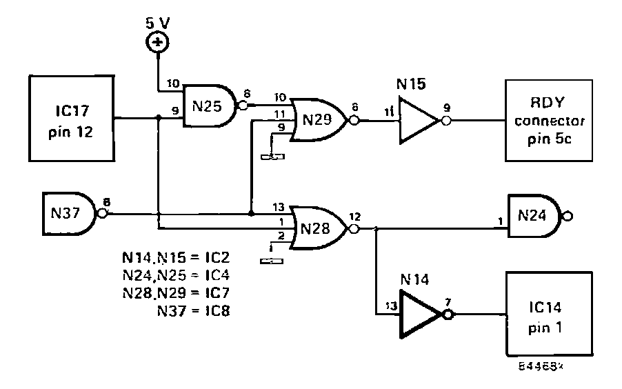
IC17 pin 12 is the Display Enable signal (DEN) from the 6845.
IC8 pin 8 (N37) is the address decoder output, active low for the 2K video memory space.
When the display is enabled and the CPU tries to access the video RAM, it will be told to wait (RDY goes false).
N28 now ensures that the 6845 always has access to video RAM when display is enabled, and the CPU has access at all other times.
I note that DEN is high for about 40 microseconds per line. This is a fairly long time, unlike the fine-grained Phi-2 interleaving on the BBC micro. A more sophisticated circuit might try to interleave access.
Elektor july/august 1984
Screen-noise killer for the VDU card with the CMOS Junior
The VDU card published in Elektor number 101, September 1983, sometimes lets noise appear on the screen, such as when a program is being listed. This fault can easily be remedied by means of a few gates in the VDU card that are unused in the Junior Computer/VDU card combination.
The trick of the circuit consists of stopping the processor when it attempts to write to the video RAM during the display enable time.
Only the 65C02 can be stopped during writing so this circuit operates exclusively with Junior Computers equipped with the CMOS Processor.
This procedure causes a slight delay in the output of a program but this is hardly noticeable in practice.
In order to carry out the modification the following IC pins on the VDU card are bent out to the side so that they are no longer in the IC sockets:
IC2 pins 7, 9, 11 and 13
IC4 pins 1, 8, 9 and 10
IC7 pins 1, 8, 9, 10, 11, 12, and 13
IC8 pin 8
IC17 pin 1.
These pins are then connected together as indicated by the heavy lines in the circuit diagram.
Pin 1 of IC17 simply remains open, while pin 2 of IC7 is already connected to ground.
Note that pin 1 of IC14 and pin 12 of IC17 must remain pushed into their respective sockets even after wires are soldered onto them.
Another possible 'extra' for the VDU card is to show a frame on the monitor within which all the video data is displayed. All this requires is a single 1k resistor connected between pin 5 of IC17 and the collector of T1.
Discussions
Become a Hackaday.io Member
Create an account to leave a comment. Already have an account? Log In.