 Joe Wingbermuehle
Background
Making a computer out of 7400-series logic, FPGAs, or PLDs is fun, but a lot of the complexity hides in those integrated circuits and their structure significantly affects any design that uses them. This led me to design and build a computer on perf-board out of NPN transistors between 2008 and 2011 (the Q1). In the end, I was left with a functioning transistor computer, but with a somewhat less than inspired design that would be extremely difficult to improve or replicate.
Today (2021), the situation has changed quite a bit from when the Q1 was built. While designing a custom integrated circuit is probably still beyond the reach of most, it is now fairly easy to get a PCB both fabricated and assembled. This means that designing and building a transistor computer is no longer such a labor-intensive endeavor. In some respects, I feel like putting this many transistors on a PCB is like designing an integrated circuit with a really big feature size.
The Q2 is my attempt at a single-board transistor computer. It is a 12-bit design with a bit-serial ALU. It is no coincidence that the architecture is similar to the PDP-8. In designing a transistor computer like this, the design decisions of old computers start to make a lot more sense.
Technology
The Q2 is implemented in NMOS using n-channel MOSFETs with resistor pull-ups. The current design uses 1094 2N7002 transistors. To reduce the transistor count and power usage, the Q2 runs at 80 kHz. The low-power requirement allows it to draw well under 500 mA at 5V, making it possible to use a USB-B connector for power.
User Interface
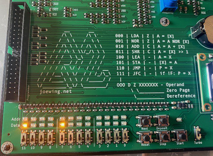
Programming is accomplished via a front-panel interface on the lower left side of the board. The front-panel has 12 LEDs to show the current address and 12 LEDs to show the data bus. There are also 12 switches to serve as inputs and the following buttons:
- Reset - Set P (the program counter/current address) to the value in the switches and reset the Q2.
- Halt - Stop the clock.
- Run - Start the clock.
- Deposit - Store the value in the switches to the current address.
- Next - Increment P.
The front-panel switches are exposed to a 40-pin header allowing the use of a Raspberry Pi for programming, which is much more convenient.
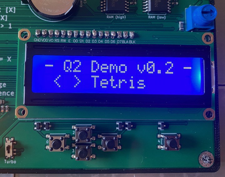
For interaction with running programs, the lower right side of the board has a 16x2 LCD that can be written at address 0xFFF (bit 8 determines if the write is a command or data). There are also 5 buttons under the LCD, whose state can be read from 0xFFF.
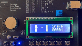
Here is a snake game:
Memory
The Q2 uses two 6264 SRAMs for main memory leaving 4 bits unused. A CR2032 battery is used for backup. The use of an SRAM IC might be controversial, but there aren't a whole lot of viable options. Making a DRAM out of transistors would be possible, and with large capacitors it might even be essentially non-volatile, but to have 12-bits of address space would use more transistors than the Q2 has. A core memory would also be neat, but I don't know an easy way of sourcing one.
All 12 bits of the address space are mapped to SRAM except for the last address (0xFFF), which is for I/O. This means there are 4095 words of SRAM total. This seemly small amount actually provides enough to do quite a bit. The snake game shown above only uses a small fraction of the available memory.
Instruction Set
Opcode | Name | F | Description
------ | ---- | - | --------------
 000   | LDA  | Z | A = [X]
 001   | NOR  | Z | A = A NOR [X]
 010   | ADD  | C | A = A + [X]
 011   | SHR  | C | A = [X] >> 1
 100   | LEA  | - | A = X
 101   | STA  | - | [X] = A
 110   | JMP  | - | P = X
 111   | JFC  | - | if !F: P = X
  |
 OOO D Z XXXXXXX - Operand
      \ \_________ Zero Page
       \__________ Dereference
The instruction format of the Q2 is identical to that of the PDP-8 with 3 bits for an opcode, 1 bit to indicate indirection, 1 bit to indicate zero page, and 7 bits for an operand address. The effective address is formed by loading the low 7-bits from the instruction and then filling the high bits from the program counter (if the zero page bit is clear) or with zeros (if the zero page bit is set). If the dereference bit is set, the word at that address is then loaded (providing indirect access).
More details here: https://joewing.net/projects/q2/
Design and Construction
The Q2 was designed in KiCad. The PCB is 2 layers 314mm x 240mm, fabricated and assembled by JLCPCB.