 Alexander Williams
As mentioned in my previous post, I've changed the way the resistors are wired in v.05 of this module. Below I'll breakdown the RS485 schematic sub-section and explain how I did things this time around.
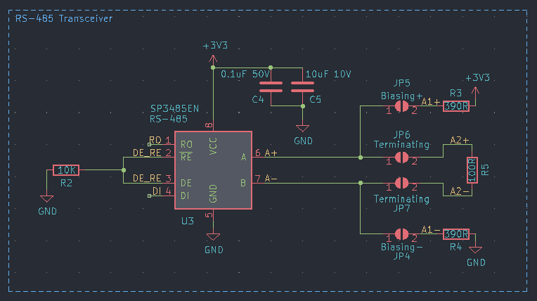
From left to right, I used a 10K pull-down resistor (R2) on the DE/RE pins, which are tied together for simplicity. This value is strong enough to bring the pins LOW, yet weak enough to bring them HIGH if you time them to 3.3V (can be controlled by an MCU pin).
The RS485 IC (U3), a MaxLinear SP3485EN SOIC-8 pin chip is featured in the middle. You can also see two ceramic non-polarized decoupling capacitors (C4, C5) routed to 3.3V and GND. The capacitor voltages have been derated by more than 50%.
Next we have the A and B pins for the RS485 differential signal. I labeled the nets A+ and A-, as this allows me to route differential traces to the RJ45 (8P8C) connector pins 2 and 1. The RJ45 connector pin 2 is routed to the A+ net, and pin 1 is routed to the A- net.
For fail-safe biasing, there is a solder jumper (JP5, JP4) routed to the pins 6 and 7 respectively on the RS485 IC (U3). Pin 2 on the jumpers are wired to 390Ω resistors (R3, R4). I also labeled the nets A1+ and A1- to make things easier in KiCad's PCB Editor.
Finally, for terminating, there is also a solder jumper (JP6, JP7) routed to the pins 6 and 7 respectively on the RS485 IC (U3). Pin 2 on the jumpers are wired to the same 100Ω terminating resistor (R5). With this size resistor and the IC running at 3.3V, it should be sufficient to create a differential voltage greater than 200mV.
The solder jumpers are pads on the bottom (back) of the PCB. Each jumper has 2 pads separated by a little space. A small blob of solder can be used to join the two pads and create a connection, thus closing the circuit and enabling the resistors. It's important to join both biasing solder jumpers, or none at all. It's also important to join both terminating solder jumpers, or none at all.
For a typical use-case, you would join all four (4) solder jumpers on the first end node (JP4, JP5, JP6, JP7). Then, you would only join the terminating solder jumpers (JP6, JP7) on the other end node. Every other node in between would not need any solder jumpers connected - since the bus will be properly terminated and biased.
The reason solder jumpers are used is because they require very little board space, and they're easy to solder together (compared to soldering tiny resistors). Also, once the jumpers are enabled, you typically don't need to change or disable them. This was a much better alternative to using a 4-position DIP switch or 2.54mm through-hole jumper headers. The cost of the resistors is so low that it made sense to simply populate every board with them, even if they won't be used.
Next, I will attempt a SPICE simulation before ordering the prototype batch of v.05 PCBs.
Stay tuned!
Discussions
Become a Hackaday.io Member
Create an account to leave a comment. Already have an account? Log In.