(work in progress...)
Introduction
Is the design of a 68000 single board computer (SBC) difficult? If you see the huge chip (dip 64) you should think so, but it is relatively simple. Compared to other CPU's like the Intel 8086, the address and data-lines are all directly available. Boards with 8086 CPU needs several latches to demultiplex the address and databus, and extra chips means extra wires.
For a simple design you need to connect all the address-lines of the CPU to the address-lines of the ROM and RAM, dito with the datelines. Besides that, a couple of logic chips will complete the design.
In this chapter I explain how I designed the SBC; I hope this will inspire you to build a SBC also, wether is is 68000, 6502 or Z80!
Design goals
The design had to be simple (KISS/keep it simple, stupid); a minimum of chips but "by the book". It should run a pascal compiler I was writing:
- 64/128K SRAM (that should be enough; DRAM is to complicated).
- EPROM for BIOS/start up, size doesn't matter.
- UART for simple but fast input/ouput (no VDI).
- VIA for timer interrupts and basic input/output.
- No bus-buffers.
- No keyboard / floppy disk / harddisk / sound / video card etc.
I read a couple of books and magazines I found about this subject and took what I liked.
Memory map
The MC68000 cpu needs ROM at startup at address 0x0000 till 0x0007 for stack pointer initiation and program start address. On the other hand the (interrupt)vectors are located in the first 1 KB, which you like to be in RAM-memory. But hey, KISS we decided, so the ROMs are at 0x0000and the vectors are fixed!
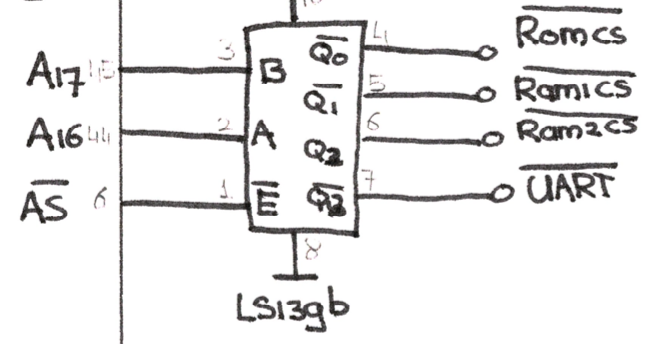
A 74LS139 demultiplexer gives you 4 banks for ROM/RAM/IO. The popular 62256 SRAM's are 8 x 32K large so every bank has a size of 64K. (Remember that the data-bus is 16 bits wide, so you always need two ROM chips and two (or four) RAM-chips).
| Bank | Address | Function | Chip | Size |
| 0. | 0x0.0000 - 0x0.7FFF 0x0.0000 - 0x03FFF | EPROM EEPROM | 2x 27C128 2x 28AT64 | 2x 16KB 2x 8KB |
| 1. | 0x1.0000 - 0x1.FFFF | SRAM | 2x 62256 | 2x 32KB |
| 2. | 0x2.0000 - 0x2.FFFF | SRAM | 2x 62256 | 2x 32KB |
| 3. | 0x3.0000 - 0x3.001E 0x3.0001 - 0x3.0003 | VIA / IO UART | MC6522 MC6850 | 16 bytes (even bytes) 2 bytes (odd bytes) |
Power circuit
The good old and uncomplicated! 78S05 linear voltage regulator gives 1.5 Amp; more than enough for the system. Although this kind of regulators spoils a lot of energy, this is how it was done the 90's.

Reset circuit
The CPU has two lines (/HALT and /RESET) which has to be asserted for at least 100 mSec at startup for a proper reset. A fine task for the good old 555. But the /HALT-line also is an output that signals the CPU is running. So it's better not to connect /HALT and /RESET together. That means extra glue logic (open collector inverters 74LS05) and a LED as run-indicator.


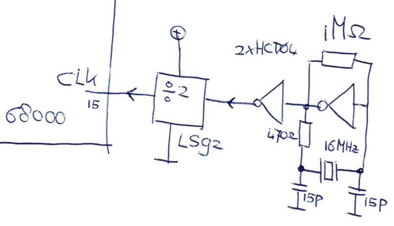
CPU clock
The CPU is running on 8MHz; to get a nice 50/50 duty cycle a divider is added, although I have seen many projects with no divider. Perhaps you can skip that part, but I used the other part of the 74LS92 also for the correct clock for the UART.
Memory decode
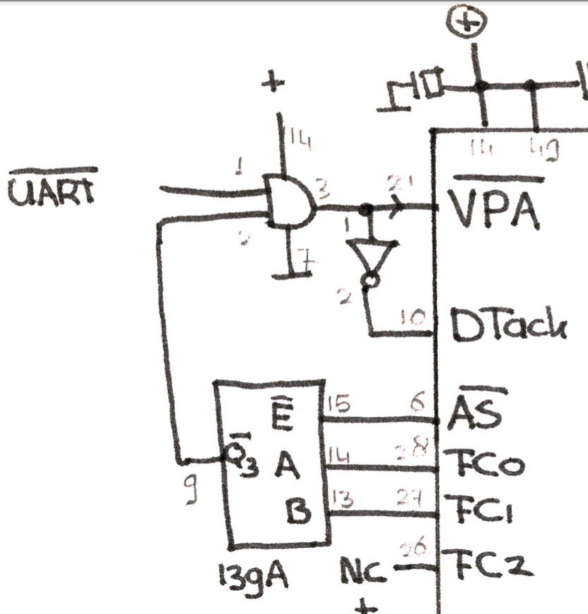
/DTACK & /VPA
The MC68000 can work asynchronous (/DTACK) and synchronous (/VPA). /DTACK is used for ROM and RAM; with this line you can add wait-states, which we don't want. (For a simple design it's better to lower the clock speed if the memory is to slow). /VPA is for MC6850 (UART) and MC6522(VIA) devices. Be aware the /DTACK and /VPA should not be asserted at the same time.
- /VPA should be low when reading/writing to the UART/VIA. It should also be low when the processor is performing an interrupt cycle. The processor expects a vector on the bus, but much easier is the initiate an auto vector. The interrupt cycle is active if /AS is low and FC0, FC1 and FC2 are all high. Luckily FC2 doesn't need to decoded.
- /DTACK should be low when reading/writing ROM and RAM, so simply invert the /VPA line.
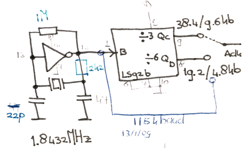
UART clock
The MC6850 has a programmable internal clock divider of 16 and 64 for asynchronous operation. Using a standard crystal of 1.8432 MHz divided by 3 or 6 (74LS92), gives us the usual baudrates. I am using hardware division of 3 and a programmable division of 16, for the comfortable speed of 38.400 baud. (The remaining 2 divider of th 74LS92 is used for the CPU-clock.)
| 74LS92 Hardware divider | UART MC6850 Programmable divide by 16 | UART MC6850 Programmable divide by 64 |
| ÷1 (B) | 115.200 Baud | (28.800 Baud) |
| ÷3 (Qc) | 38.400 Baud | 9600 Baud |
| ÷6 (Qd) | 19.200 Baud | 4800 Baud |
UART 6850
VIA 6522 (IO)
Interrupts
The MC68000 support classic 6502/6800 peripherals, and also prioritized interrupts. A 8 to 3 multiplexer connected to IPL0 / IPL1 / IPL2 gives 7 interrupt lines. But if you only need one, skip that extra chip.
Both the UART and the VIA have open collector interrupts, so these pins are connected together to IPL2 as IRQ4 with a 4K7 resistor pulled to Vcc.

RTC
SD-card