 Eric Michat
HARDWARE COMMENTS
Schematics Page 1 :
CLOCKS : The board is based on a simple Z80 architecture ; the clock is supplied by a quite classic XTAL oscillator at 4.194304MHz, which happens to be 2^22 Hz. The undivided clock is used for the Z80 itself, and the 1 second pulse, at the output of IC18 is used to provide a non-maskable interrupt (NMI) for the software RTC. We are talking about a vintage clock, so no way to use a RTC chip on this board :-) !
Of course if the power goes off, the current time is lost ; that's the charm of the design.
On the Z80 data sheet, the system clock is expected to be close to a 50% duty cycle, but in my experience, with "low" frequency operation (like 4MHz), it's not a problem, so an extra frequency divider with a toggle FlipFlop to provide an accurate 50% duty cylcle is not mandatory.
ADDRESS DECODING : IC4B provides a simple address decoding for the RAM and the ROM. The ROM starts at 0x0000 and ends at 0x7FFF ; the RAM is the space left from 0x8000 to 0xFFFF. Of course, it's 50 times the need for our application !
IC4A provides the I/O decoding for the 3x 8-bit latches and the buffer input. The 256 adresses available in the I/O space of the Z80 are therefore divided in 4 pages with multiple duplications, but it's not an issue as long as we don't need to add extra I/O devices.
POWER ON RESET : IC19 was a well known PO Reset circuit in the 90' and ensure a "clean" start-up condition. It's better than a simple RC network, but it can alos do the job.
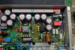
Schematics Page 2 :
OUTPUT BUFFERS : 3x output latches are required to drive 6x BCD to decimal decoders ; it's important to use BCD-TO-DECIMAL decoders that have an OFF state of all outputs above 0d9 code (to turn off all the Nixies cathodes). Not all decoders provide this function. It's also important to have high state drivers because we use N-Channel MOS to drive the Nixie tubes (see later).
Schematics Page 3 :
BOOST CONVERTER : The Nixie tubes require a 180V DC drive voltage and for the IN18 types, about 4mA per tube is expected. So we need a DC step-up converter (non isolated) being able to provide 180V at 25mA at least. This function is built arround IC8 TL497, which was a quite standard PWM controller in those years. An external N-Channel MOSFET is used with a classical boost architecture topology based arround L1/D2/C15. This part is the most "tricky" to manage. Of course, there are thousands of more efficient solutions to do the same function in 2021, but once again, it's a vintage design !
The converter works at low frequency (a few KHz) so commutation losses are not an issue, same for the gate drive of the MOSFET( no need to gate discharge with a gate driver).
NIGHT DIMMING : A simple photo-diode is used to reduce the converter voltage for night operation. So when the photo-diode current drops, the N-Channel transistor T63 is open and the feedback resistors R18 and R13 are no longer connected to ground, leading to a reduced output voltage (165 V for instance).
The "daylight" operation voltage (180V typ.) and the "night" operation voltage (165V) can be adjusted by means of the 10K trimers.
LOGIC POWER SUPPLY : it's definitely not possible to design a vintage board without using a linear 7805 regulator for the logic supply ! The DC 12V input helps the boost converter to operate at lower current ; the total current consumption is about 1 A, but depends mainly on the effiicincy of the boost converter. Using HCT logic instead of LS will also help to reduce power.
PUSH BUTTON INPUTS : IC16 is used to provide a simple set of 3 ON-OFF inputs for the time setting purpose by means of 3 push-buttons. RC networks ensure a basic debouncing function.
Schematics Page 4 to 6 : The use of several simple N-Channel small signal MOSFET has been prefered to High voltage integrated drivers for Nixie tubes. These components are mostly bipolar transistor arrays but limited to 60V or 70V outputs with zener protections, so they...
Read more »


 ClimbinElectronics
 Muth
Muth
 Emil J
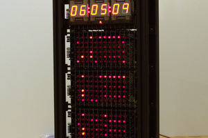
 Ted Yapo
👍 Nice piece of work, especially the case. I like your clear explanations of the design choices you made.