Introduction
I was preparing this project with other projects of mine, like this:
https://hackaday.io/project/176652-3d-printed-reflective-microscope
For be able to understand what will I talk about, I would like to introduce first some of the basics.
Basics:
In general when we talk about displays we can distinguish two main type.
The first one is Liquid Cristal Display (LCD) and the second nowadays picked up Organic Light Emitting Diode (OLED).
LCD displays:
LCD displays working principle based on light polarisation. These type of displays easier to manufacturer.
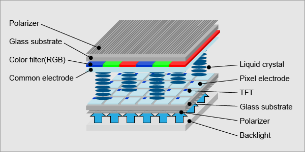
From reverse engineering point of view the most interresting layer is the Thin Film Transistor (TFT) layer, which contains most of the pixel driving electronic.

LCD displays usually contains more glass layest then the OLED displays. From left to right the part are:
cover glass; back light; color filter and on top the polariser; last but not least the TFT layer.
The LCD display control a diplay driver IC which controls both the DATA and SCAN lines. The vertical lines usually the DATA lines and the horizontal lines are the SCAN lines. My main interres was how manufacturers can make such a small edge around the active area of the display. If you think about this the usual mobile phone display has more than 1000-4000 vertical pixels, but the edge of the display is not more than a millimeter or two.
The answer to this they use shift registers to scan through the whole vertical pixels. This methode is quite smart, whit this they only need a couple of control signals and the rest is handled by the logic.
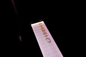
In the below picture you can see the active pixel area, marked red. Next to it left is the edge of the display where the SCAN shifting logic takes place. For reference this is an Iphone 5 diplay TFT layer.

For reverse engineering I have used my DIY reflective microscope with 20X objective. Below you can see the earlier marked area in magnified view. Do not be confused, I have took several small pictures (100x100 micrometer) and stiched them manualy. It took me a couple of hours to stich more than 100 picture together and part of that you see three 1134 number, because I have only captured ones the 1134 line. The SCAN circuits are the same apart from the addressing, but for easier understanding I have stiched multiple SCAN drives next to each other.

I have tried to figure it out how the transistors and the control signals connected. Made a small circuit diagram in EASY EDA, it is not perfect because in reality the FETs does not have diodes connected to them, so please ignore those.

OLED displays:
OLED display logic driving is simillar compared to LCD, but the fundamental difference the OLED pixels need current driving till for the LCD enough voltage driving.
I have got an Samsung S8 plus screen which I am gone analize. On the picture below you can see phisicaly the OLED display has less layers but over áll the complexity of those are much higher, especialy the tft layer. On the right side you can see the tft and on top of that thw orgabic layer. The left side has the cathode, touch layer and the cover glass.

My main focus here also was the row pixel driving circuit (scan lines), which are takes place on the very edge of the display around 1mm wide. This circuit fundamentaly work the same way as on the LCD display it has shift registers which scans through the rows one after an other. The complecity comes from the current driving which for Samsung displays has pixel driving compensation circuit as well.
To be able to see the better the tft layer of the display I had to etch away the top metal layer, which was the sub-pixel anode contacts and on the scan drive curcuit had a metal mesh shilding possibly. On the next two picture width are 100um across the image, just for scale.
Sub-pixel cathode contact:

Scan drive curcuit under the metal shielding:

After etching away the metal layer you can see the...
Read more »
 Daniel
Cool. You need to cooperate with @Arsenijs on this thing: https://hackaday.io/project/179868-all-about-laptop-display-reuse