Close
0%
0%

High voltage differential probe

This project is about a differential probe for voltages up to 400V. The voltage ratio is 1:10 or 1:100.

Similar projects worth following
Target of this project was to develope a differential probe for voltages up to 400V with the following specs:
Accuracy: about 1 %
Bandwith: ~100 MHz
Switch between 1:10 and 1:100 ratio for measuring voltages
Input impedance: 6 MOhm and 1,67 pF (per input)
Be careful with voltages over 60V-DC and 25V-AC! If you use this probe with higher voltages you should know what you are doing!
You need an isolated supply for the probe with 12..18V DC (100mA)

I started with a design of Andrew Levido that you can find it in the links below.
Then I adjusted parts until it fits my requirements.

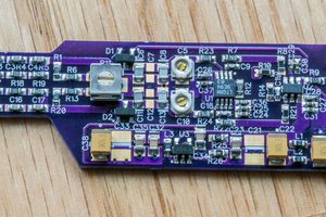
The first step was to change the frontend from four to six resistors and capacitors in series. I wanted to use SMD Parts and 1206 is a good available size. But to get enough voltage strength four parts in series is a bit small. With 1206 parts you can use 1,5mm gaps wich is great for the creeping distance.

The second step was the supply of the probe. I don't want a battery because in my experience it's always empty when I need it. So I decided to use a barrel jack input. I added a capacitance multiplier and a LDO-regulator for filtering, a bigger voltage range and reverse polarity protection (LT1129). I got the LT1129 cheap from eBay, else it's a bit expensive. With a 12V supply I get about 10,5V for the op-amp wich divides the supply in +/-5,25V. I got the idea from Bud Bennett's project (https://hackaday.io/project/169390-a-10x-100mhz-differential-probe). The probe should also work with 15V or 18V. If the voltage is to high the LT1129 will protect itself with its overtemperature protection up to a voltage of 30V.

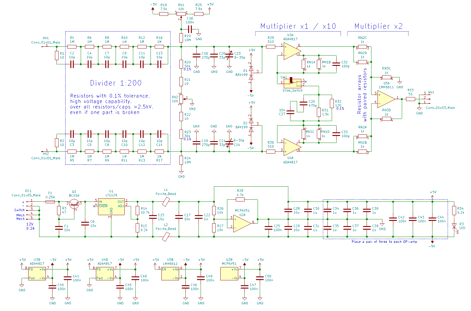
-> Schematic completed, you can find it below beside the BOM.

Now it was time to think about the connection of the HV-input and the BNC-output. I decided to use safety banana-plugs, that are specified for 1000V. For easier connection I didn't use sockets, but wires with the plugs at the end. The same decision was made with the BNC connector.

The next step was the layout. There were multiple things to observe. At first the frontend should be routed symetrically. Then the ADA4817 has layout hints (like no ground plane under the op), that must be followed. The LMH6611 is not that critical, but the complete analog circuit must be free of interference. The last part is the supply which should be as wide away from the rest as possible. For low impedances I used a plane for ground (but not under the ADA4817), another one for +5V and one for -5V. Also important for safety reasons are the cuts in the PCB, that increase the creeping distance in the frontend. All in all it should be enough for 230V AC (but use it on your own risk!).

-> You can find the layout and the gerber files blow.

Update: LT1129 footprint is wrong, should be TO-263 (D2Pak), but is TO-252 (DPAK)

Update 06/02/2021: Pin assignment of the BAV199 diodes is wrong

Update 06/06/2021: Two capacitors were not connected correctly

The 3D case is now ready for download. I developed it with FreeCAD and printed it with a creality ender 3 printer and PETG material. Be careful with the switch, it must be soldered very accurate to fit through the hole. I added a picture in the gallery with the case.

06/02/2021 Update: Added a hole for the LED and some deepenings for the trim potentiometers.

06/07/2021 Update: First working prototype, i made some hotfixes against the mistakes above. Schematic and layout are now fixed, resulting in V1.1

06/12/2021 Update: I changed the case a little bit. The height was increased about 1mm so that no parts are touched by the case. The four mounting holes are now perfectly for M3 16mm flat head screws.

Case_T-Body.stl

Case top

Standard Tesselated Geometry - 2.39 MB - 06/08/2021 at 19:09

Download

Layout.PNG

Layout preview V1.1

Portable Network Graphics (PNG) - 263.86 kB - 06/07/2021 at 21:57

Preview
Download

Adobe Portable Document Format - 84.16 kB - 06/07/2021 at 21:54

Preview
Download

sheet - 11.49 kB - 06/07/2021 at 21:52

Download

Case_B-Body.stl

Case bottom

Standard Tesselated Geometry - 2.85 MB - 06/02/2021 at 20:24

Download

View all 6 files

  • Installation, callibration, first tests

    SiMi06/12/2021 at 15:40 0 comments

    At first an isolated power supply with 12V DC (could be up to 18V, about 60mA) needs to be connected to the barrel jack. The LED should now light up. It's a good idea to check here if the supplies +5 / GND / -5V are correct.

    The callibration consists of three steps:

    1. CMRR (Common mode rejection ratio): Deactivating the offset calibration by shorting C16 (alternatively: Set RV1 so that Pin2 of RV1 is on GND). Now connect a high voltage source to both HV inputs. I recommend 60V, because this is high enough and save. The negative pole of the source need to be connected to GND. Now measure the voltage difference behind the frontend between the both branches. You can use Pin3 of the diodes D1 and D2. Change RV2 to minimize the voltage. Remove the shorting of C16.

    2. DC-offset: Connect both HV-inputs together. Measure the output voltage e.g. at R33 to GND. Change RV1 to minimize the output voltage. By changing the switch between 1:10 / 1:100 attenuation you will see, that the output voltage will change. At the end find a good compromise between both switch positions.

    3. Adjust frequency compensation: Similar to passive probes there exists also a frequency compensation C23/C24. Use the 1kHz square wave callibration signal of your oscilloscope and connect it to one HV input. The other HV input must be connected to the oscilloscope GND. Set the probe to 1:10. Now use the corresponding capacitance trimmer to adjust the frequency compensation. You have the correct setting if you have no over- or undershoot.

    First test:

    The 1kHz rectangular test signal of my Rigol oszi (DS1052E) has only frequency shares up to about 100kHz, so at first I decided to use my 140V source with relais as test source. I compared the signals with a passive Rigol RP2200 (1:10 setting, 150MHz bandwith) and an active differential probe TT-SI9110 (1:100 setting, 100MHz bandwith).

    1. DIY probe (CH1) vs RP2200 (CH2), 40V relais pulse:

    2. DIY probe (CH1) vs TT-9110 (CH2), 140V relais pulse:

    The results look very promising. The probe has less delay, as the Testec probe. The frequency compensetion is not perfect (first peak is lower than with other probes), the trimmer capacitor reached the limit. I have to lower C20/C21 to 27pF. The tested frequencys were in the range up to about 12MHz and the probe has no problem to handle them.

    Just for interest, the complete turn on process of the relais in the source at 40V (DIY probe (CH1) vs RP2200 (CH2), 40V relais pulse (20us/div):

View project log

Enjoy this project?

Share

Discussions

parasole999 wrote 06/01/2023 at 10:15 point

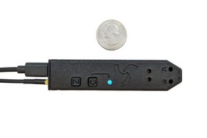
Hi there and thanks for posting your probe variant!  Question if there is a way you may post PCB Kicad project?

  Are you sure? yes | no

Similar Projects

Does this project spark your interest?

Become a member to follow this project and never miss any updates