 Eric Hertz
No joke, it seems I was spot-on about the unused pins.
So, yes, indeed, I /could/ wire up the new FLASH to use 128K above the RAM, call it "RAM pages 8-15"... Add a tiny bit of glue logic on its and the RAM's /ChipSelects...
OR, I could wire up the Flash's chip-select to... Duhn duhn duhhhnnn... The Z80-ish's unused /Chip-Select2 or /Chip-Select3. Piggybacked atop the built-in ROM, we're talking two bodge-wires (/CS2, and /OE... from somewhere... heck, I could use /CS3 /for/ its /OE), and no need for glue logic, nor popping pins of other devices. Heck, even /WE is there to be piggybacked.
Anyhow, I was also right about the two additional address bits. This thing's designed to map in four devices each up to 1MB. 4MB! WOW!
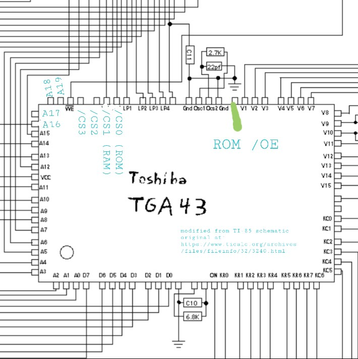
And, something weird... U10 is unpopulated and bypassed with a zero-ohm resistor at "S4." U10 appears to be a one-gang 2-input OR(?), its inputs tied to /CS0 (the ROM's chip select) and /CS3 (which is selected by writing both bits 6 and 7 high in port 5 or 6). Its output is connected to the ROM, at its chip-select. So, apparently, for some reason they had the ability to map the ROM from two places(?). This /Almost/ sounds like my idea for bodging-in the seemingly non-existant (and necessary for FLASH writing) /OE. Huh.
I tried, a little, to figure out the /OE pin they /did/ wire to the ROM; it's so near the LCD signals and so far from anything else bus-related, I thought maybe disabling the LCD would toggle that pin, a wild hack on their part... but, nah, nothing I did turned it off (it seems it never goes high). wait...? ... no... not even selecting a different device in the "ROM" page... right? Wait, did I do my tests with port 5 or 6? Hmmm. Gah, I wonder if it's an extra bit on the "link port" which just happens to never be written high...
Anyhow, there are /plenty/ of options with 3.625MB of unused address space to work with!
...
The Display: The T6A40 row-driver on the back of the LCD does, indeed, toggle its carry-output. That means it's receiving more than 68 clock pulses. This looks good for my display-hack-for-general-purpose-outputs idea. Though, the thought occurred that the default address for the frame buffer, being at 0xfc00, causes the legit pixel data to end at 0xffff. IF I'm right about the display driver's continuing to spit out RAM data during lines 65-68 (and, obviously above), then where's it getting it from? I tried disabling interrupts, so nothing was running from the ROM, and... I didn't see any ROM chip-selects... so it's not wrapping to the Z80's address zero. Is it possible it works with the RAM's addresses, directly? Then, Oh Wait. The framebuffer mapping port, as I recall, adds C000 to whatever value you put in for the high address byte... C000, of course, being the beginning of the permanently-mapped RAM page 0. So, it probably wraps to RAM-address 0 = z80-0xC000. Duh. That, unfortunately, would be much harder to check with only a logic probe... though, actually, having been an oscilloscope guy from an early age, I'm quite pleasantly surprised with how much can be determined with nothing but a logic probe and a different way of thinking. Maybe I'll come up with something, if I decide to go that route. (I've got a 'scope I love in storage).
One thought for a /use/ for this idea is quite simply snagging a second identical display, maybe find an otherwise busted TI-86 somewhere, and daisychain them, vertically. Most-likely the '86 isn't outputting 68+64 rows, maybe only a handful more, even, but... even tapping those 4 extra rows could be handy for, say, status icons. I /think/ the display could even function after being cut with a glass cutter... something I've wanted to try for quite some time... making use of the still-usable portion of old cracked displays.
Other ideas have been described in past logs, adding a shift-register (or 7) to snag that data and turn it into outputs. Not really necessary, now, with two unused chip-selects, and 2 unused address bits, heh!
...
Am I forgetting anything?
I /think/ I may've figured out the memory-cleared problem...
If you cut the power when a program is running, even a BASIC program, you get a mem-clear. Oddly, if you cut the power when your program is running through AsmIDE86, you get "Memory Recovered". How does it know? I dunno. But, i did read something about its having some crash-protection. Smart...
Especially because I messed up my understanding of the timer interrupt, LCD-disabling, and keyboard stuff... which results in an infinite loop only breakable by cutting the power.
THAT was the big savior of the project-momentum, finding out that "Memory Recovered" worked with my bug... I had ZERO energy for trying to figure /that/ out. This was about figuring out those pins, and figure them out I did! WEEE!
What a day! There was a time nearly all my days were nearly as productive/fruitful, now it's a *very* rare occasion. This is one to be remembered... maybe even immortalized in solder.
4 MEGABYTES!!!
Whatcha gonna do with all that junk up in that trunk?
F Y I. In case anyone forgot... This is a TI-86 I'm working with, but the same processor VLSI, Toshiba T6A43, is used in the TI-81 and TI-85, as well. I dunno what they got inside 'em, but snagging signals from PLCC's (e.g. this guy's ROM) isn't too difficult. Get hacking, yo! I wanna see a soundblaster or SID or HP-IB or something in one of these guys!
Oh yeah... so port 5 and port6... they map the extra memory pages (16KB, each) into the Z80's address ranges 0x4000-0x7fff and 0x8000-0xbfff, respectively. They seem to work the same. Bits 7 and 6 choose one of the four chip-selects (In a sense, Bit7 and Bit6 are A21 and A20, but those've been decoded for us into 4 separate active-low chip-selects). Bits 5-0 select the page within the selected chip... They basically are written to the A19-A14 pins, along with the chip-select, whenever the Z80 tries to access 0x4000-0xbfff.
...
Holy schmoly... This page woulda been handy...
http://diolum.free.fr/projets/TI-86/OLD-TI-86.html
(Lookie there! I got an achievement award for being the first to submit it to archive.org!)
TODO: COMPARE FINDINGS
Of note, from a quick-scan: S4 allegedly goes to /OE, and their device appears to have a FLASH where I have an OTP. Which would seem to confirm my theory that writing the FLASH ROM on the devel system was accomplished by accessing it via /CS3. Now, I was pretty certain I traced S4 to the ROM's /CE, but if that was on the /other/ side of S4, that'd make sense, I think. E.G. U10 ORs the T6A43's /CS0 and /CS3 (the OR is actually an AND since the inputs and outputs are Low-true). That's sent to the FLASH's /CE input. Thus the FLASH can be accessed identically at both chip-selects' addresses. Now, maybe, the FLASH's /OE is wired directly to /CS0... Then, for read-only purposes, that'd do great. And then when /CS3 is selected, /OE (/CS0) is high... which is necessary only for /writing/ to the FLASH. Bam. I think. But, I coulda sworn I see /my/ /OE tied to another pin, which seems always low... so why didn't they just ground it? One thought: maybe it goes high when the T6A43 is in low-power mode. But, that's what I thought before, thus testing the LCD Off port settings. I see a couple other possibilities, undocumented bits in PORT4, for instance. But, if they had that, they coulda just as easily used it for writing the FLASH... Except, maybe, as a preventative measure to prevent accidental flash-writes...? I dunno.
Discussions
Become a Hackaday.io Member
Create an account to leave a comment. Already have an account? Log In.
remarkable find on the French site
"I know it's not cool for the heritage but it is not in working order"
"Dead hard drive = loss of data and motivation = End of reverse engineering" -- lolz been there, done that
Are you sure? yes | no
hah, yeah!
Are you sure? yes | no