 Eric Hertz
well... I mean... really... If you consider the T6A43 Z80 VLSI as a bit of a microcontroller, and if it were officially documented... then the only real "hack" I did, circuit-wise, was figure out a way around its lack of an Output-Enable on the I/O bus.
Toshiba's "hack", therein, was apparently to not assign a pin to it, despite its being de-facto on the Z80 inside. Assuming, I guess, most RAM/ROM chips don't really need it. It, from the devices I've checked, (TI's RAM, ROM, and my vague memories of most other such-interfaced memories I've used in the past), can be tied active in most cases, wherein ChipEnable does the job of preventing output, and WriteEnable overrides output. There may be a little room for bus contention during the brief period between enabling the chip and loading the data to be written before the device can disable its output in response to WriteEnable... but, probably minor, and maybe even moot due e.g. to the propagation-time for output in the first place. OK, I think I can buy it as a design intent.
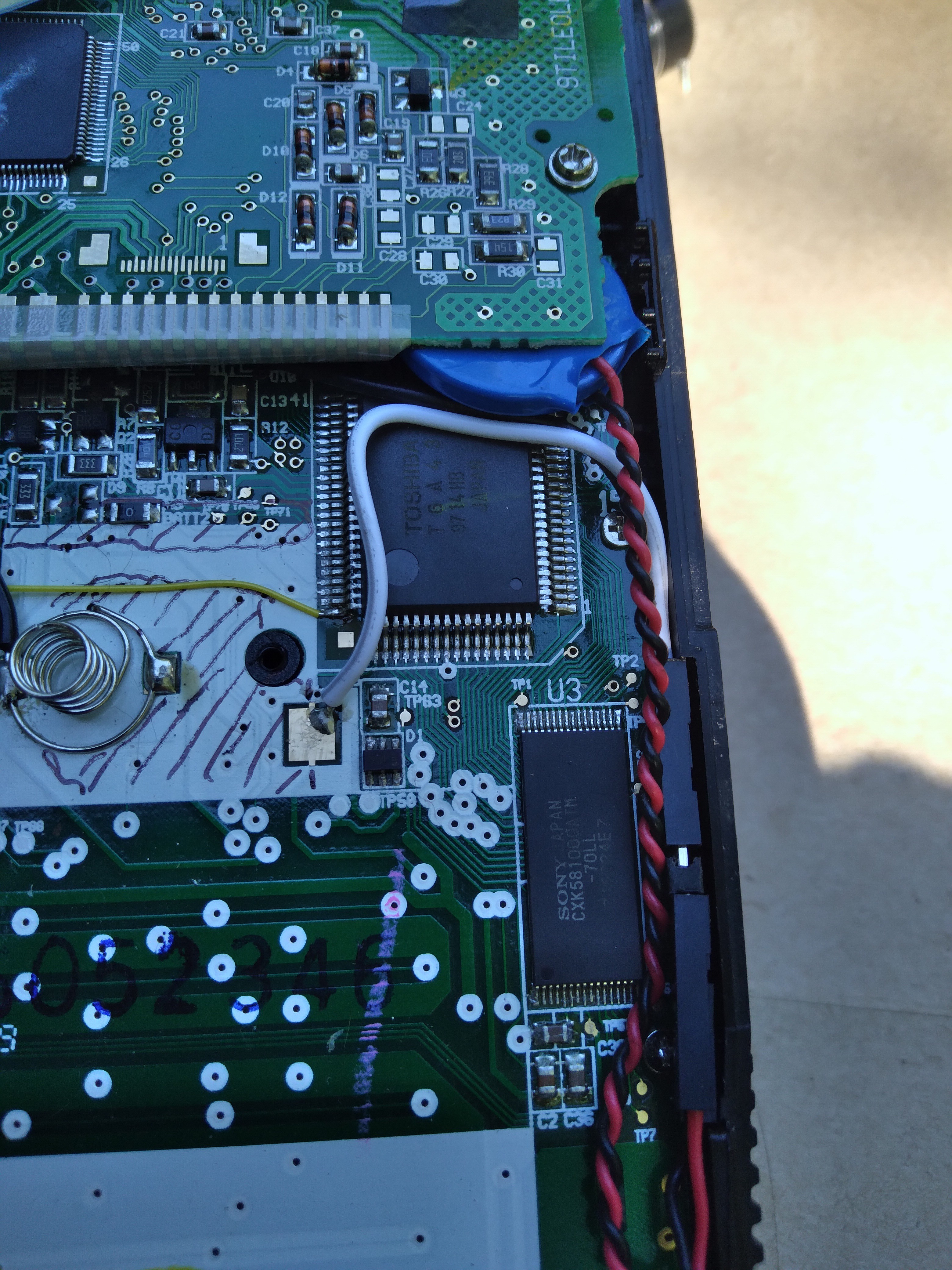
TI's "hack" was similar to mine, it seems, in how to drive the /OE on the FLASH chip they apparently used during devel of the TI-86... That chip differs from the others, in that /OE must be inactive to enable writing. No /OE, most devices' /OEs being constantly active... now what? Yesterday I linked a page which, as I recall, shows /OE coming from some logic fed by Chip-Enable 3. But I've reverified my board's traces, and I don't see /OE anywhere but the ROM and a strangely-located pin on the T6A43. I watched it with a logic probe under many conditions and never saw it change. Which makes sense if it's a hack for the FLASH (which mine doesn't have, an OTP ROM in its place, instead), but of course would /not/ make sense if it really was the Z80's /OE. (It'd toggle with RAM accesses!)
So, I've yet to find its source in software, but it very well may be nothing but a currently-undocumented general purpose output e.g. from an unused bit on the link port. And, of course, we never see any other value on that bit nor pin other than 0, because my ROM/OS version is designed to be run from an OTP PROM.
My '86, however, /does/ have an unpopulated IC that looks to select the ROM (or FLASH, in the devel edition) when /either/ CS0 or CS3 is selected. So, my thought is they used /CS3 when writing the FLASH and /CS0 to run code from it. (HMMM, but if OE is disabled /during/ a /CS0 access, say to execute the code to program the flash, then nothing would come through! This doesn't make sense! Presumably they'd run that code from RAM... with Zero ROM function-calls... but if they did that, then /CS3 would be unnecessary! Unless, maybe, internally the VLSI blocks WriteEnable with /CS0? Huh. The other guy's makes more sense... use CS3 AS Output Enable).
Anyhow, I opted for similar in my only "real hack" in this endeavor of adding 256K of FLASH. I assigned A18 to Output Enable.
OH OH OH OH! HAH! More on that in a bit.
I'd originally planned to use /CS2 for reads and /CS3 for writes. Then /CS3 would be directly-wired to /OE. Badda-bing.
(Double HAH! Somehow I'd missed that I'd have to OR /CS3 and /CS2 to go to its ChipEnable input!)
But, I decided, instead, kinda late in the process that I didn't want to waste a dedicated Chip Select which could be used in another add-on.
So, I decided to wire-up A18 to /OE... and since /CS3 was already broken-out to the unpopulated IC's pads, I used it for my FLASH's Chip Enable. Great! Now the FLASH looks like 512k instead of 256 to the Z80 VLSI... one half is read-only, the other half is that same data, at the same locations in the chip itself, but write-only. Great! That works for my needs... and it's not like 256k of extra address-space usage is a big deal. Heck, it'd've been occupied anyhow, without additional address-decode logic. And there's still a whole 1MB left with /CS2.
Heh, so coming back to the big shock I had earlier... Using a chip-select for /OE meant my read-addresses would be the lower addresses and write-addresses higher, which kinda makes sense to me intuitively. It hadn't occurred to me when switching the design to Output Enable on A18 that now the lower addresses are write only, and the higher addresses read-only. That's kinda weird. But, we're not booting from this, so no biggy... it all gets mapped into 0x4000 or 0x8000 either way, anyhow.
So, I guess that's the only "real hack" I did... The rest is pretty commonplace... I'd always wanted to do a "piggyback" project, now I have... and on a PLCC, rather'n a DIP, no less! Hard Core!
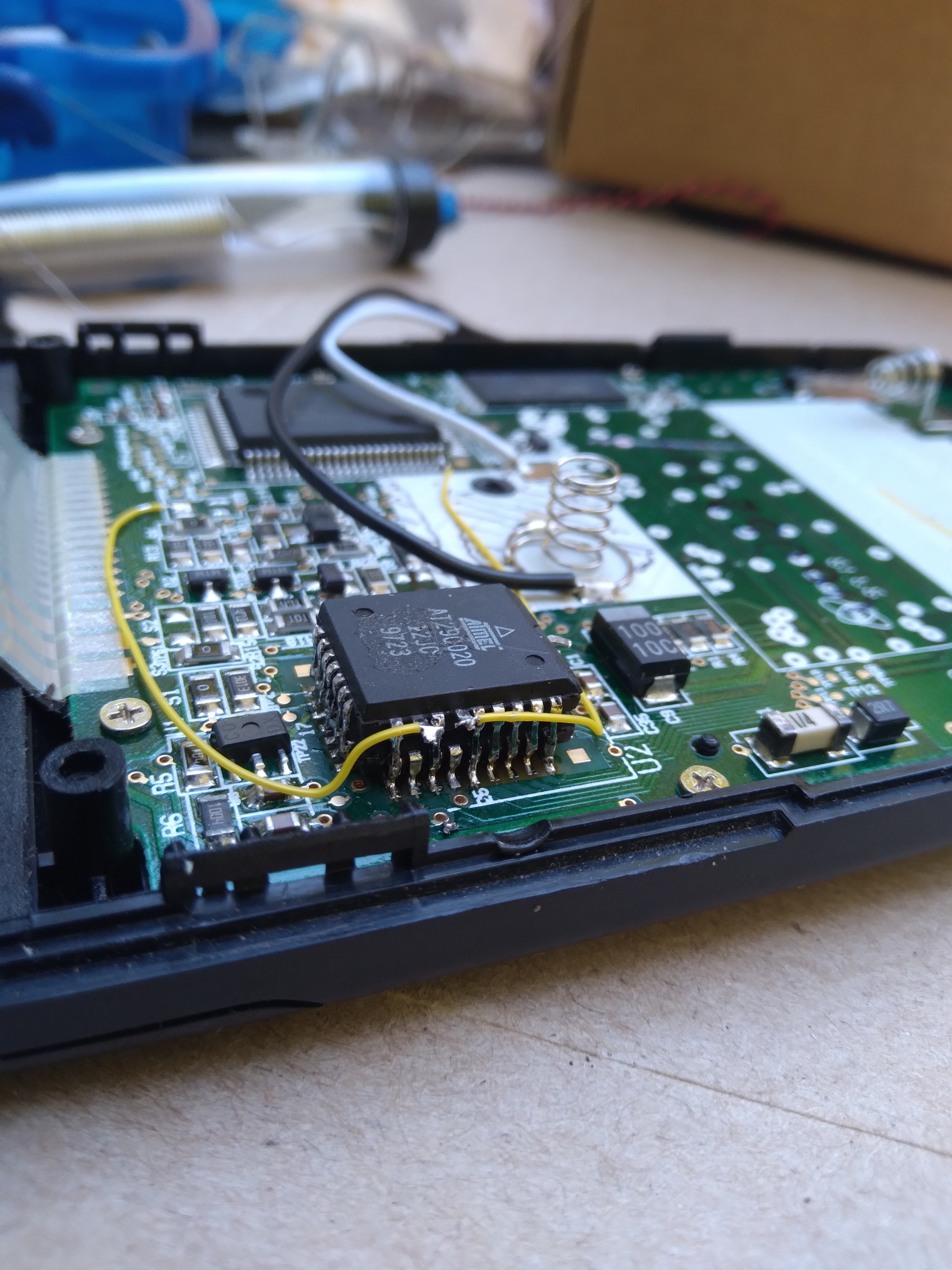
It's almost like TI designed it with this in mind... there's about 1mm clearance if you allow the legs of the top PLCC to stand atop the shoulders of the other. But, I splayed them out a bit so the top chip is belly-to-back with the other; leaving room for wires, etc. in case I need to tap off the bus for something else later.
(Yes, I'm soldering at a picnic bench in a state park... yes, I get a lot of weird looks... no, I wouldn't recommend it, if you've got other options. But, it's a nice day! And good shade, and way better than soldering in my tight fishbowl quarters where I'd be getting even weirder looks, and fumes, etc.! Overall, pretty stoked (aka grateful)).
And in another one of those satisfying moments when two things never intended to be together fit together perfectly (actually, /two/ here!):
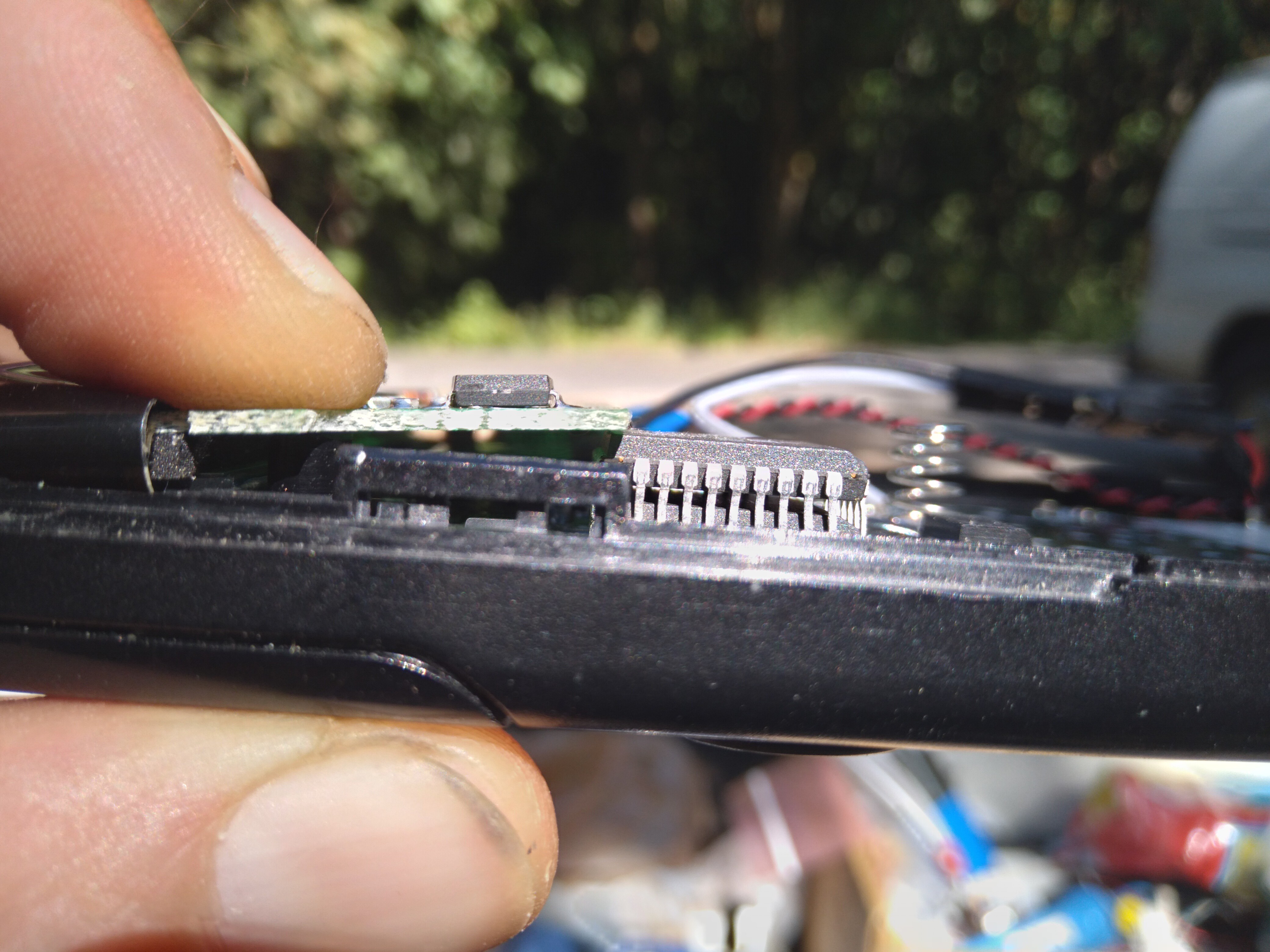
The connectors for the internal battery fit perfectly between the PCB, the case, the clip for the back of the case, and the little indent where the sliding cover slides on. That extra header sticking out between the two connectors is due to a long header, the connectors are squeezed together tight. Perfect Fit. Crazy.
And, of course, the battery which fits perfectly under the LCD board... doesn't even need anything to hold it in place. The wire that protrudes from the coin cell slides in between the CPU in such a way that if rotated afterwards it holds in place gently but not rattlingly... and the springiness of the wire, along with the position of the connectors, causes it to prevent rotating again to fall out. I mean, seriously. What is that thing called...? Two things fitting together perfectly almost as if designed to.
Overall, an /amazing/ couple days, luck-wise. Could things be looking up?
......
LOL. A18 is LOW for Lower addresses. /OE is Active Low. Lower addresses have the outputs enabled... for... READ. LOL. Just as I'd've preferred. My brain, sometimes...
Now, frankly, some of this "luck," lately, is a bit unnerving... but maybe this time I'll try not to jinx it by being too skeptical. The other method hadn't done me well for many years.
Discussions
Become a Hackaday.io Member
Create an account to leave a comment. Already have an account? Log In.