 zaphod
In the last project log I mentioned that I encountered some hardware bugs that required solving. They were:
- mechanical strain on the main electrical assembly occasionally caused the display to stop working
- changing the wire that connects the main oscillator to the FPGA results in the clock not ticking any more
Solving problem 1
I initially suspected that this was due to a cold solder somewhere in the connections between the micro and the LCD, but after much reflowing of solder joints and continuity testing I couldn't find the problem.
Eventually, I just started desperately trying to see if any of the LCD data lines were connected to ground by accident, and this actually turned up a result. After some more hunting I found the source of the problem.
Instead of using proper standoffs I was using a nut and some washers to get the main PCB at the right height off of the power supply as shown in this image:
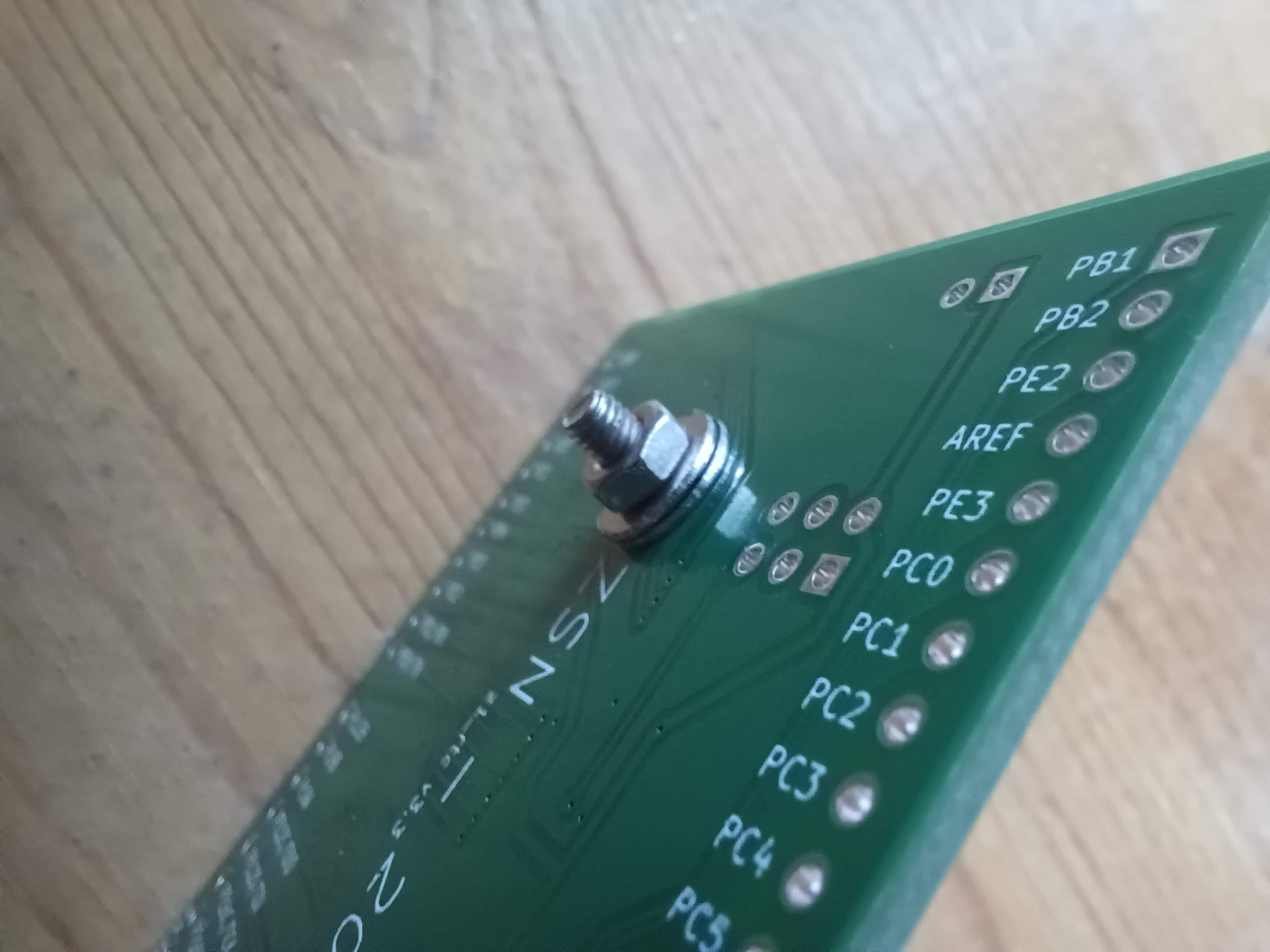
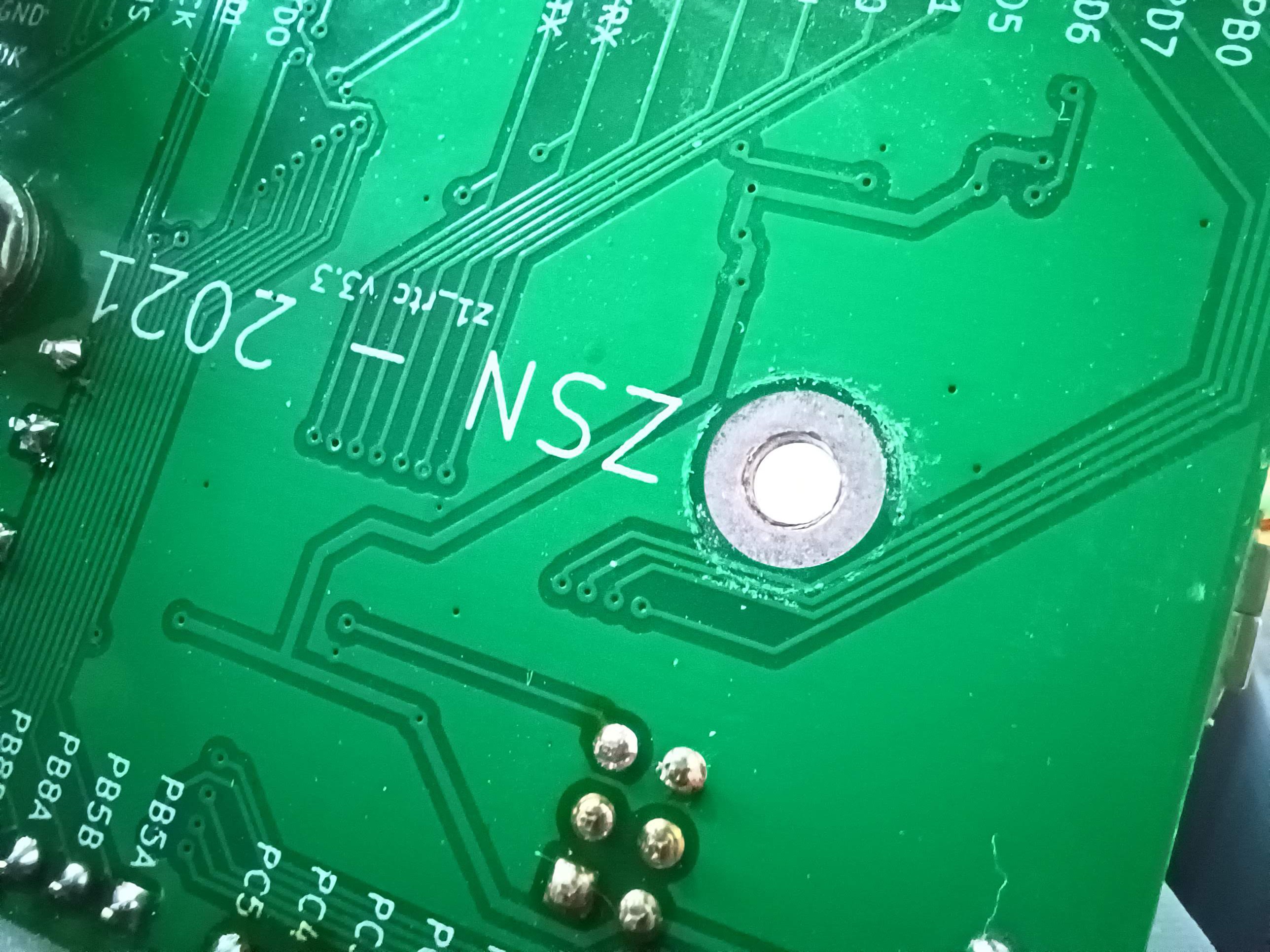
and it turns out that the edge of the washer was slightly sharp and larger than the plating around KiCad's default M3 hole. Furthermore, I had an LCD data line routed next to the mounting hole, and so the washer had cut through the soldermask on both the ground plane and the signal line and managed to just barely bridge the two. here's a picture showing the damaged soldermask where the washer was:
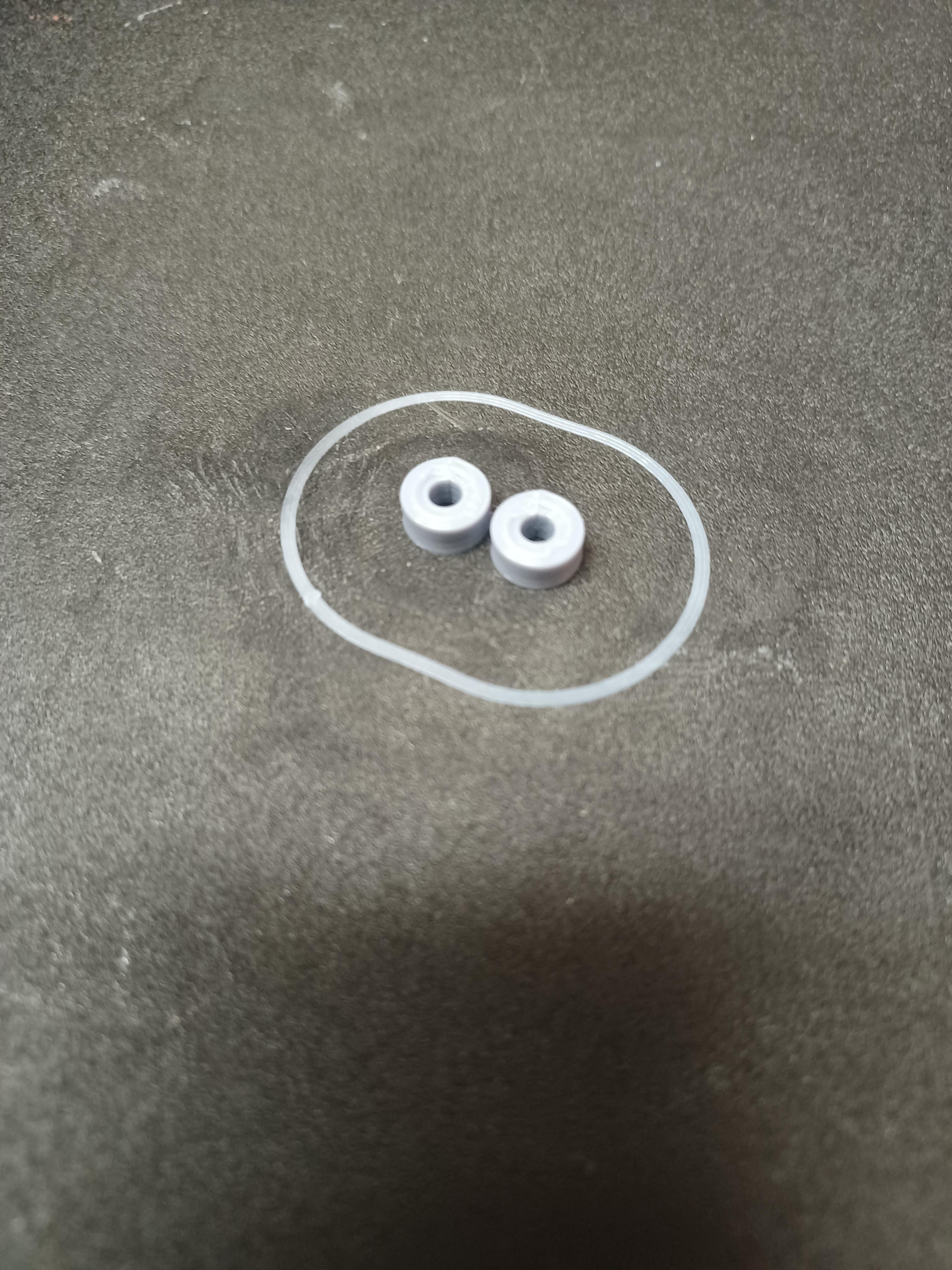
Annoyingly, this bridge was not very stable, and so the error it presented was intermittent and sometimes solved by bending electronics assembly a little, making it seem like the result of a cold solder. Once I'd discovered the source of the bug though the solution was to simply 3d print some appropriately sized standoffs:
Solving Problem 2:
Problem 2 was a lot worse. Basically I got all of the firmware working while the hardware was in an unfinished state, and part of that unfinished state was that the wire connecting the main crystal to the FPGA was just a random chunk of wire I'd soldered in.
Later when I went to replace the random wire with a shorter piece of wire with headers (to allow the main PCB to be disassembled from the oscillator) the clock stopped ticking.
Fair enough, forcing a 20MHz square wave through some 0.1" headers is probably asking a lot, so I undid the headers and just soldered in a wire, and it still didn't work. So then I went back to the initial long wire, and it also didn't work...
At this point it was clear that there was some transmission line nonsense going on that I do not have the tools to deal with, so I started getting desperate. I tried all sorts of different wires, I tried changing FPGA pins/slew rates, I tried using some shielded cable (cut out of an old USB cord), and basically nothing worked.
During testing I periodically switched back to the initial wire and every once in a while it would work again, but not always. At this point I was worried that the physical structure of the conductors was acting as a resonator or filter or something.
Out of shear desperation I decided to try replacing the 20MHz line with an SMA cable, and connect to the main PCB and the OCXO with proper SMA connectors. In the end this is what ended up working which is great! But also indicated that I really should have done better job of considering my high frequency signal path in the first place, which I mostly neglected since "20MHz isn't that fast". (a 20MHz square wave has some really high freq components though!)
Anyway, In order to get this fix working I needed to build an adapter board that would allow me to hack an SMA jack onto the main PCB, and carrier board for the OCXO that includes an SMA jack. In the end my solution looked like this:
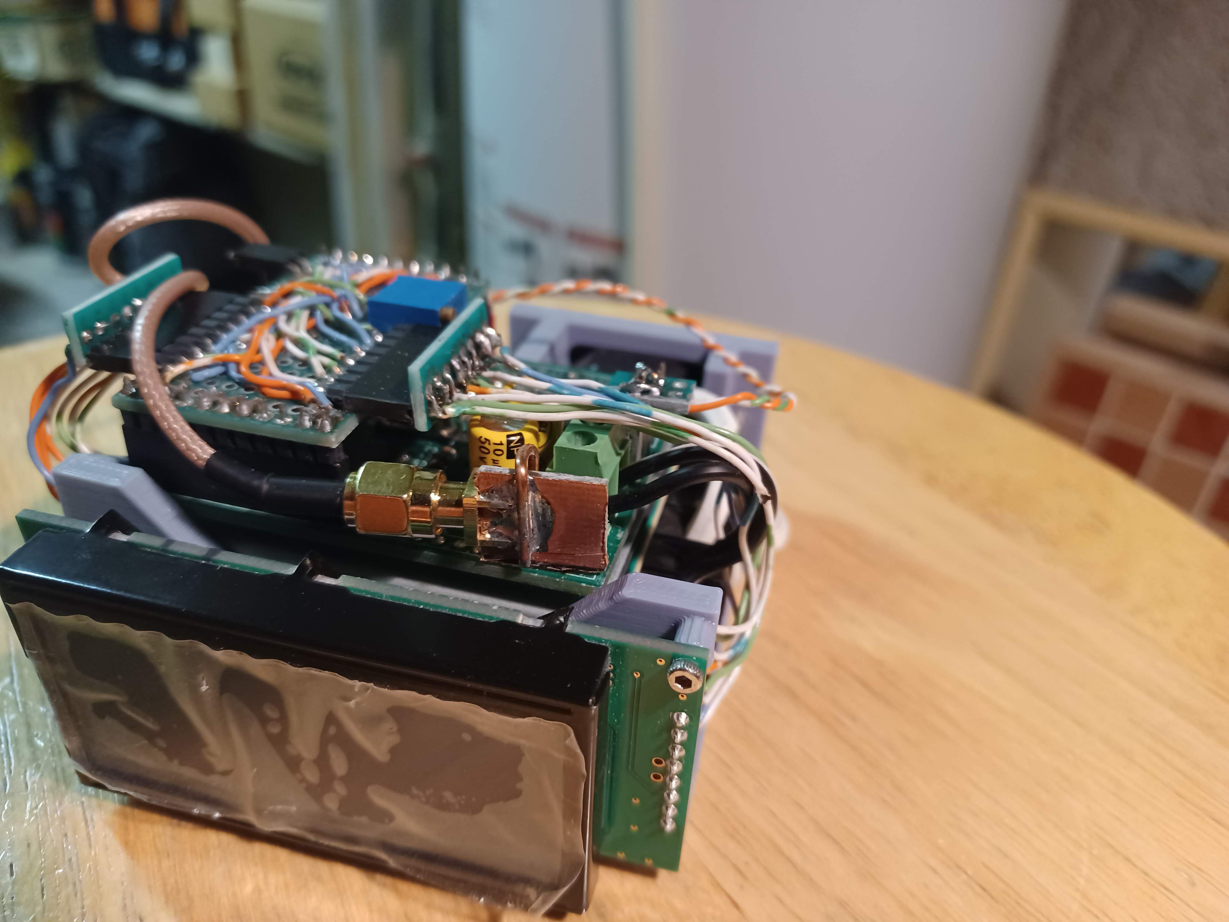
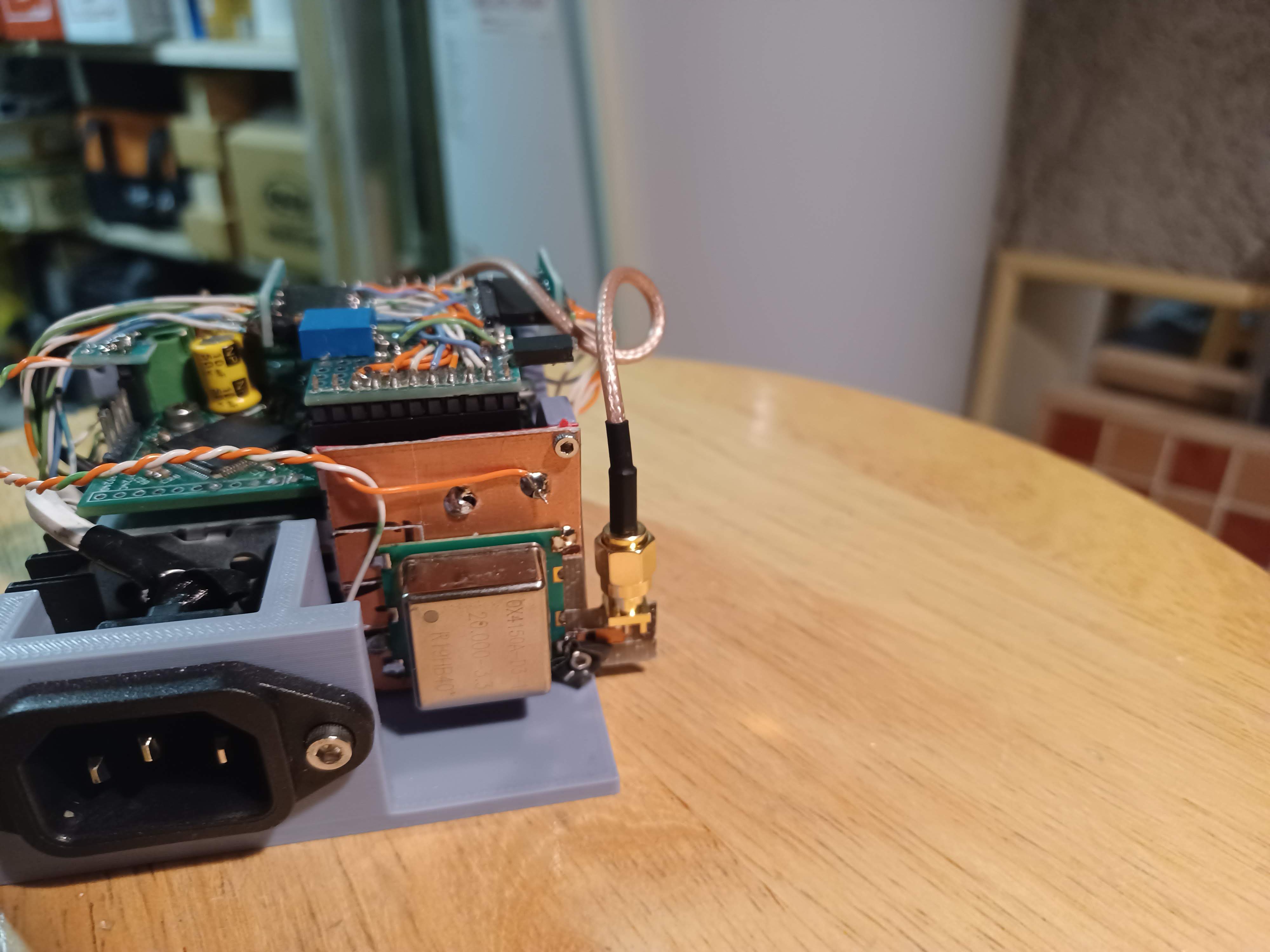
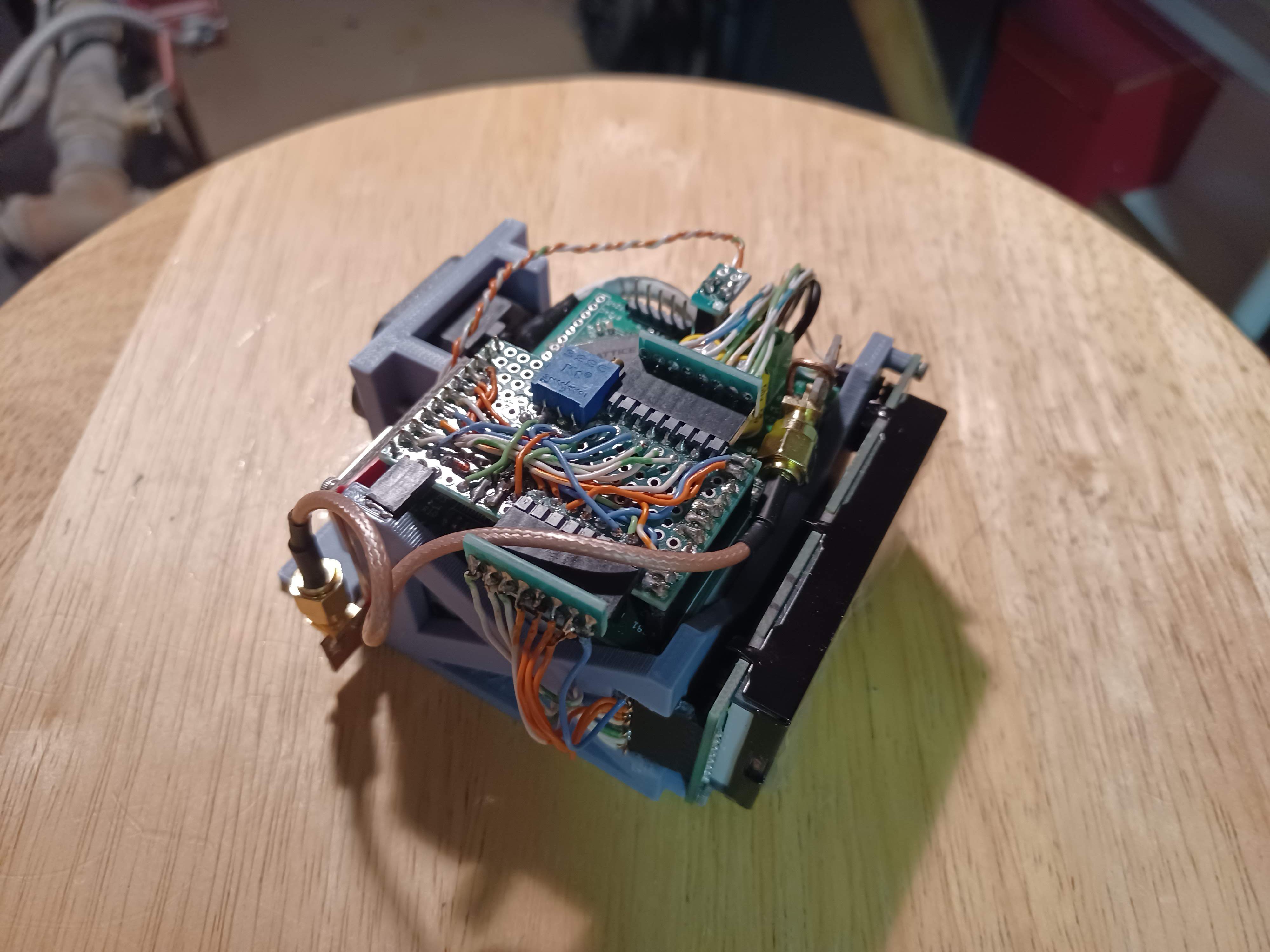
As you can see from the images above, its a bit of a hack job, but it does have some retro ham radio/diy rf vibes which makes me feel all warm and fuzzy inside.
also worth mentioning that I did try to cut the tracks that connect to the SMA jacks such that they form 50 Ohm microstrip lines to try and avoid reflections at the SMA jacks, but IDK if it helped much in the end, since the dimensions are just what I could do by hand, and IDK what the impedance of either the OCXO output or the FPGA input is.
Discussions
Become a Hackaday.io Member
Create an account to leave a comment. Already have an account? Log In.