 Aleksa
An oscilloscope's input buffer has a very odd (and strict) set of requirements. Its input impedance must be 1MΩ in parallel with about 15pF, for compatibility with standard oscilloscope probes. The front end must also take in any signal within the oscilloscope's voltage ranges and attenuate or amplify it to fit the ADC full-scale voltage. It must be able to AC or DC couple the input signal as well as terminate it in 50Ω (on higher end scopes). On top of these requirements, the front end must keep voltage noise low enough to be undetectable by the ADC as well as meeting a maximum bandwidth of 350MHz!
Rev.1
Once again taking inspiration from [bunnie & xobs'] oscilloscope module (specifically the probe schematics) I decided to use an opamp to provide the high impedance, high bandwidth part of the buffer. To spec this opamp out, I had to know what gain I needed for the system. I wanted to find the minimum gain I needed, so I used the lowest full-scale voltage on the ADC, 1.8V. I divided this by the input voltage at the lowest voltage range. I wanted the scope to be capable of 500uV/div, which with 8 divisions gives an input voltage of 4 mV peak to peak. Therefore, the maximum gain of the system was 1800mV/4mV = 450 V/V. That's a lot of gain! And since I used the resistor level shifting from the linked probe schematics, I had to double the gain to offset the resistive losses. So out of 900 V/V of gain, the PGA I wanted to use provided about 87 V/V maximum, leaving about 10x gain left for the poor buffer opamp to squeeze out. With a desired bandwidth of 350MHz, the opamp needed a gain bandwidth product of over 3.5GHz! It also needed a high impedance input, very low noise and a blazing fast slew rate.
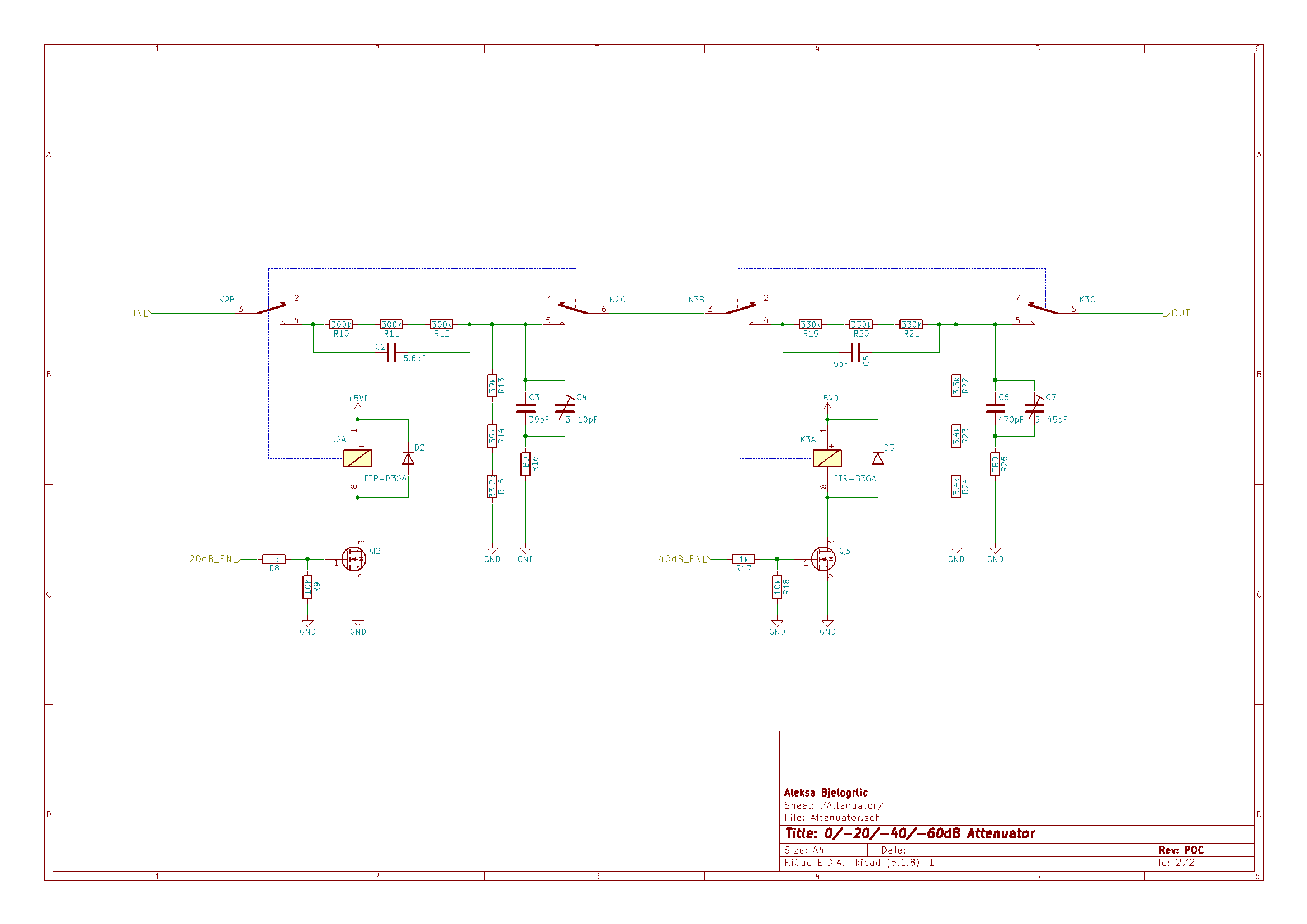
A parametric search left me with only one opamp that was up to the challenge, the LTC6268-10. This ticking time bomb of BOM cost had a few drawbacks other than the price tag. First of all, this part is a "de-compensated" opamp that requires a minimum gain of 10 for stability. Since a gain of 10 is needed, this is just barely stable. Second, due to the slew rate, the output voltage must remain under 0.45V peak to peak to avoid distortion due to slewing. Combining these two, the maximum input voltage was 0.45/10 = 0.045V. To work with this limitation, I designed a system of two attenuators to give 10x, 100x, and when combined, 1000x attenuation. Shown below is a spreadsheet of all the voltage ranges and how the attenuators and programmable gain amplifier (PGA) needed to be configured to meet the ADC's lowest full scale voltage of 1.8V.
With the opamp chosen, and all these requirements in mind, I booted up my trusty copy of KiCad 4 (I wasn't a Luddite, that was the latest version then!) and got to work. Below are the schematics of the first revision of the FFE. 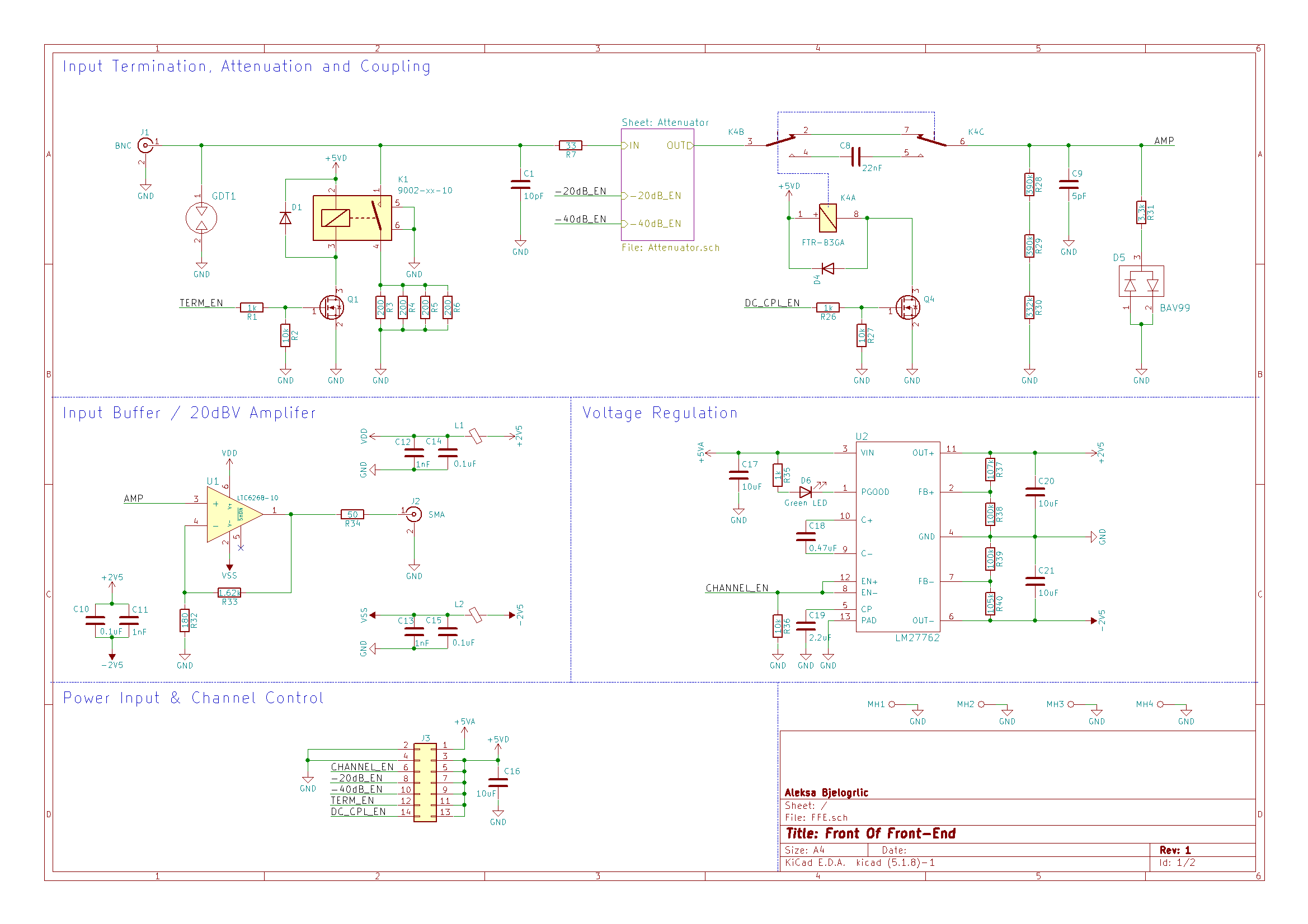
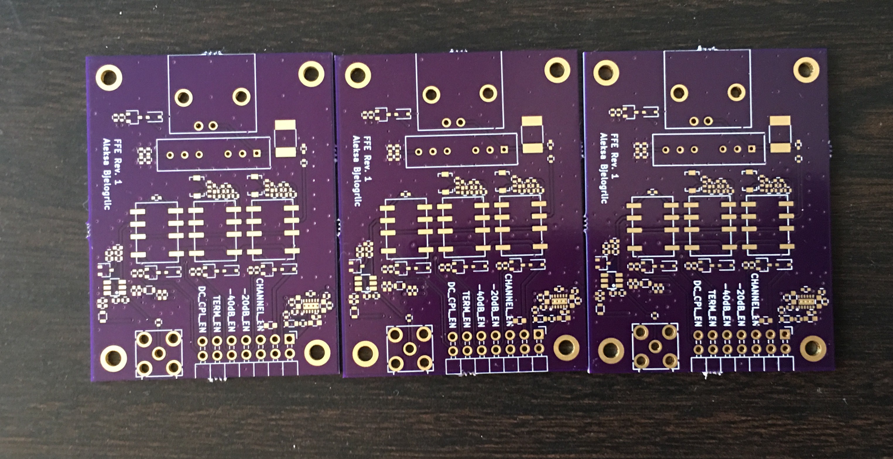
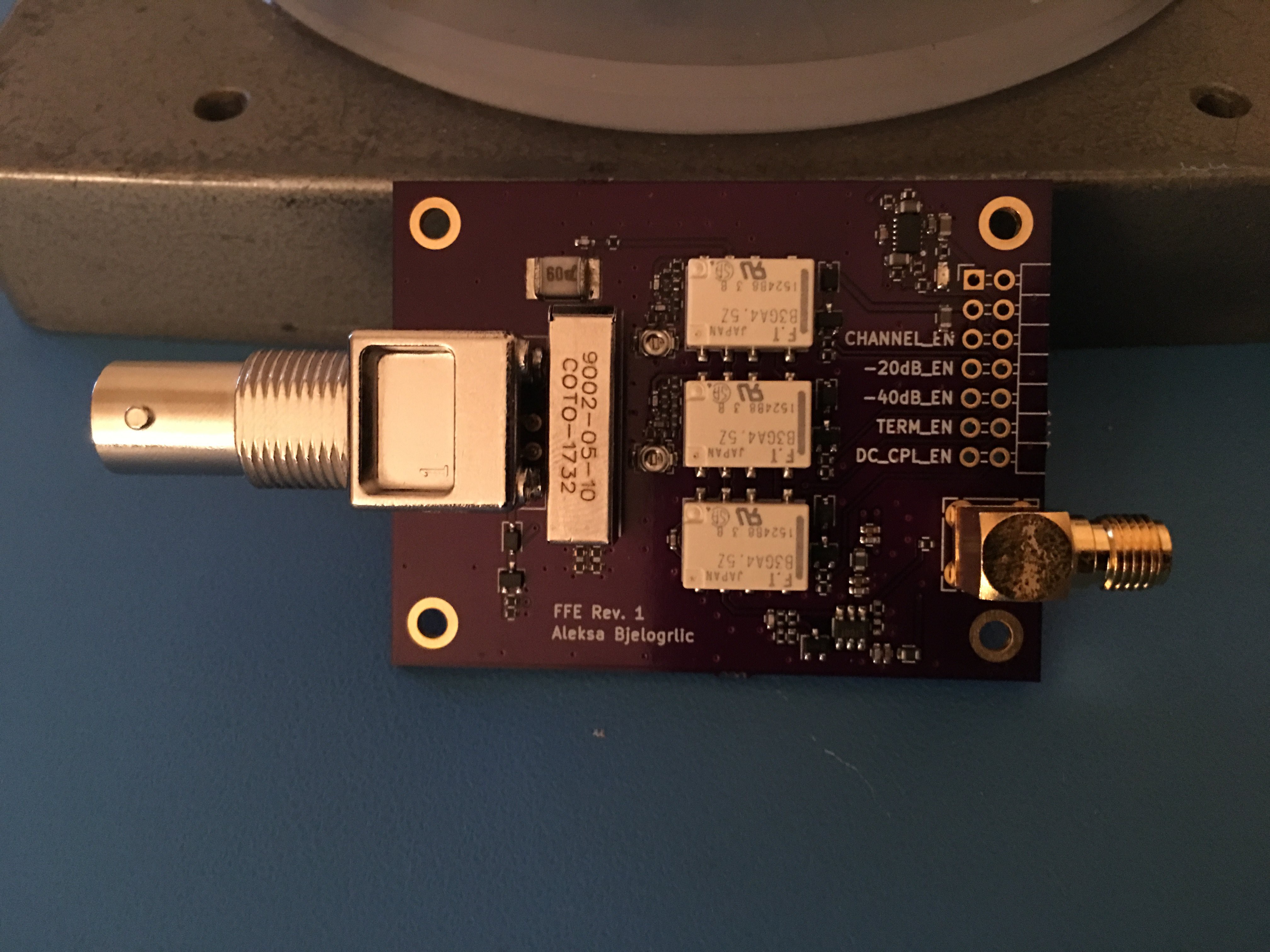
From perfect purple PCBs to potentially performant prototype - thanks to OSHpark's four layer service, aluminium stencil from OSHstencils, and an afternoon under the microscope! At the time this photo was taken, I either ordered the wrong headers or forgot to order them entirely, but who manages to make only one order for a board anyway? In my next post, I'll discuss this revision's test results, problems encountered, and a hasty band-aid solution that proved I should always get a good night's sleep before sending out a new board!
Thanks for giving this post a read, and feel free to write a comment if anything was unclear or explained poorly, so I can edit and improve the post to make things clearer!
Discussions
Become a Hackaday.io Member
Create an account to leave a comment. Already have an account? Log In.