 Aleksa
Before designing the ADC board, I made a separate adaptor board to take in four front end channels and bring them out to only one connector. This saved board area (and a lot of cost) by cutting down on the ADC board's width, giving the two boards a T-shaped profile.
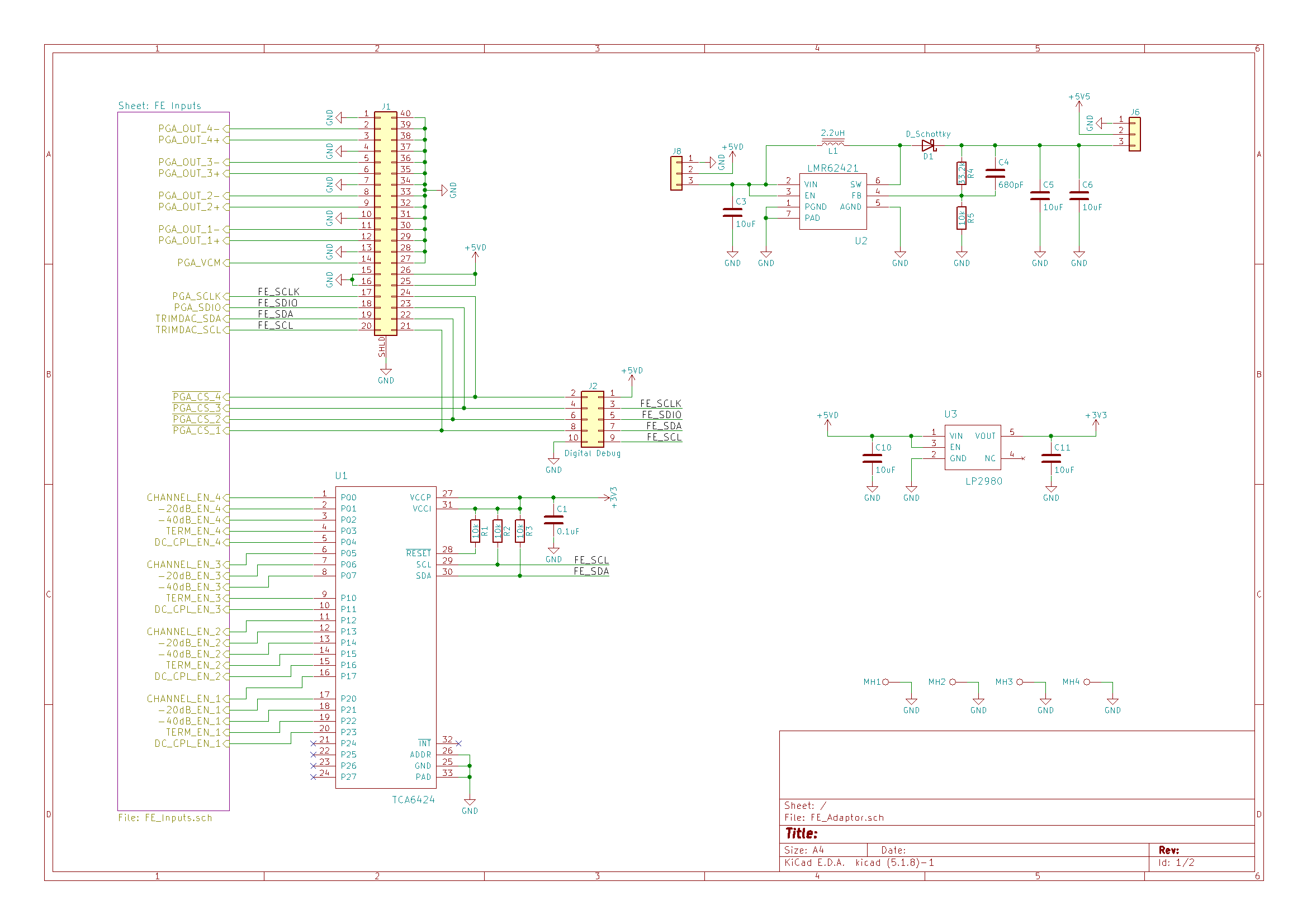
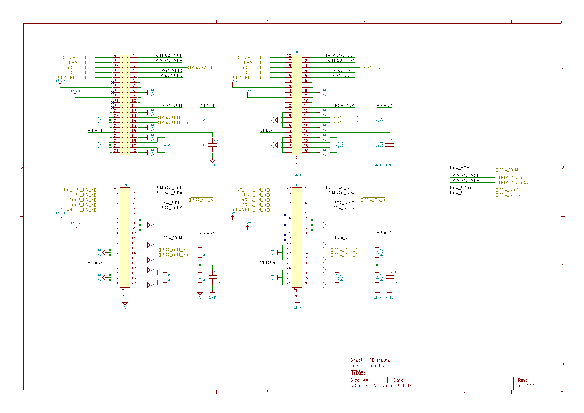
Each connection to the front ends terminated the unused AUX output of the PGA with 100Ω and set the AUX bias to mid-rail. The main outputs and bias input were routed to the ADC board connector (J1). As on the front end tester, the USB voltage was stepped up to 5.5V by a boost converter (U2) and both voltages were fed to each front end. The SPI and I2C interfaces were bused together (with separate chip selects for SPI) and routed to the connector for the ADC board as well as a debug connector (J2). An I2C GPIO expander (U1) was used to cut down on the number of connections to the rest of the system and a linear regulator (U3) was used to power it.
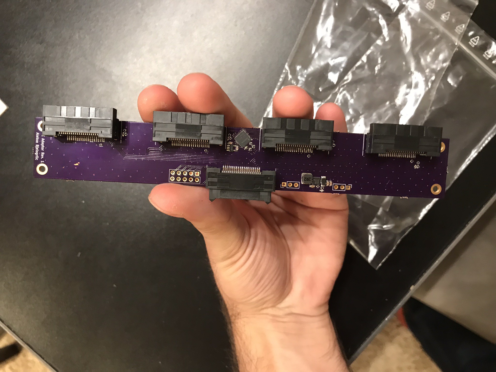
Live long and prosper, board. The poor thing almost didn't make it, since it was bigger than the hot plate I normally used to reflow solder boards with! But with enough hot air, the job was done.
ADC Board
The HMCAD1511 ADC is an amazing little chip! I initially selected it since it was the cheapest 1 GSPS ADC I could find through normal distributors. Turns out, it has lots of tricks up its sleeve, like digital gain. This chip interleaves eight internal ADCs to sample one, two, or four channels at 1 GSPS, 500 MSPS or 250 MSPS respectively. Taking Nyquist into account (with some wiggle room for filtering), this allows for 350 MHz bandwidth on one channel, 200MHz on two channels, and 100 MHz on four channels. Sampled data is output on eight DDR LVDS lanes, with a bit clock and a frame clock for synchronization. Since no line operates faster than 500 MHz, this type of output requires no special high speed transceivers, making it easy to interface with a low cost FPGA. All of these factors explain why this ADC is also used on almost every low-cost oscilloscope on the market!
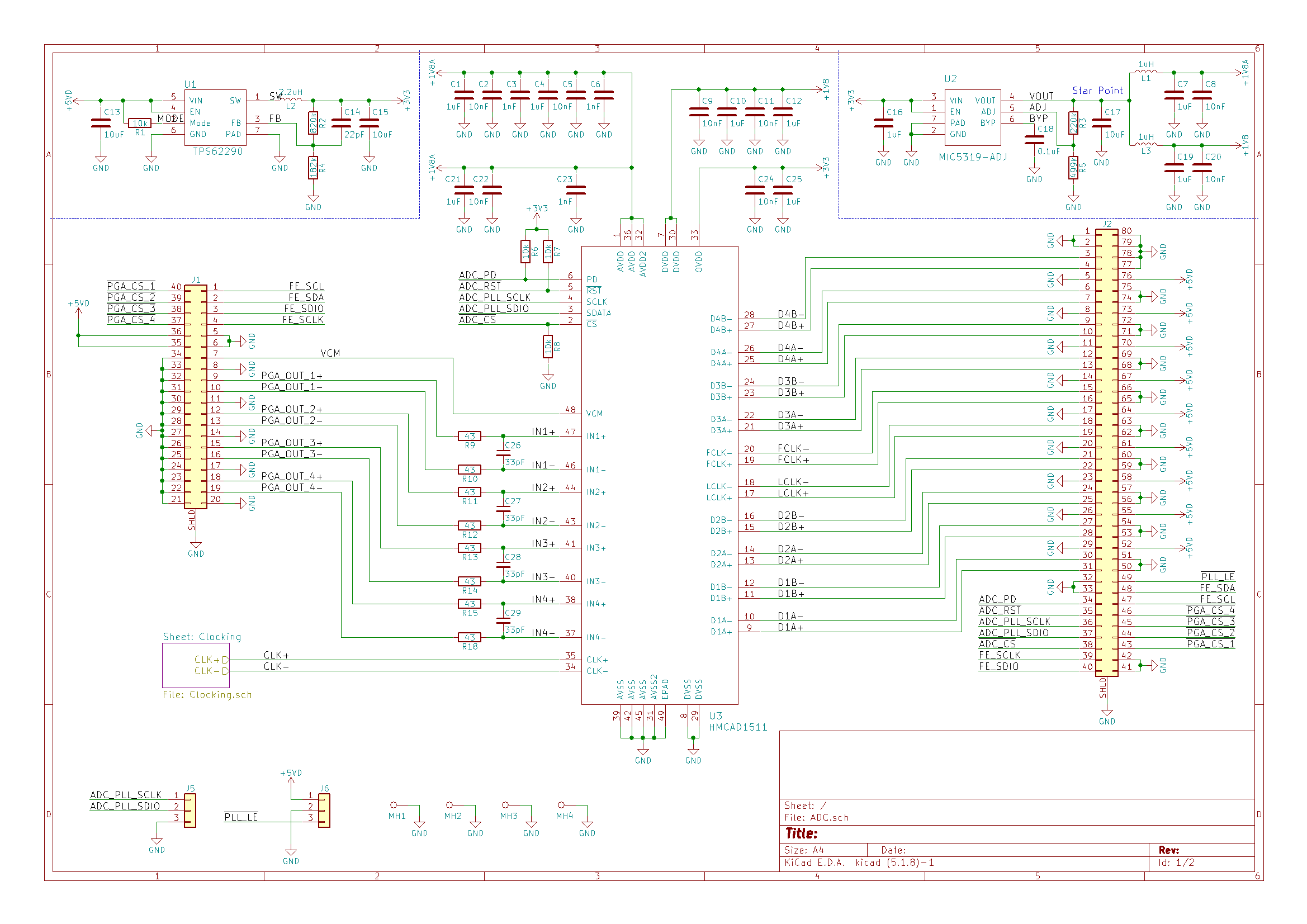
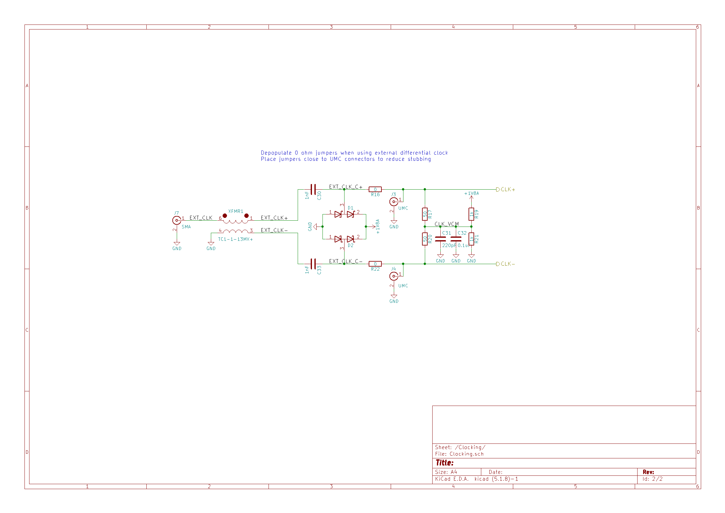
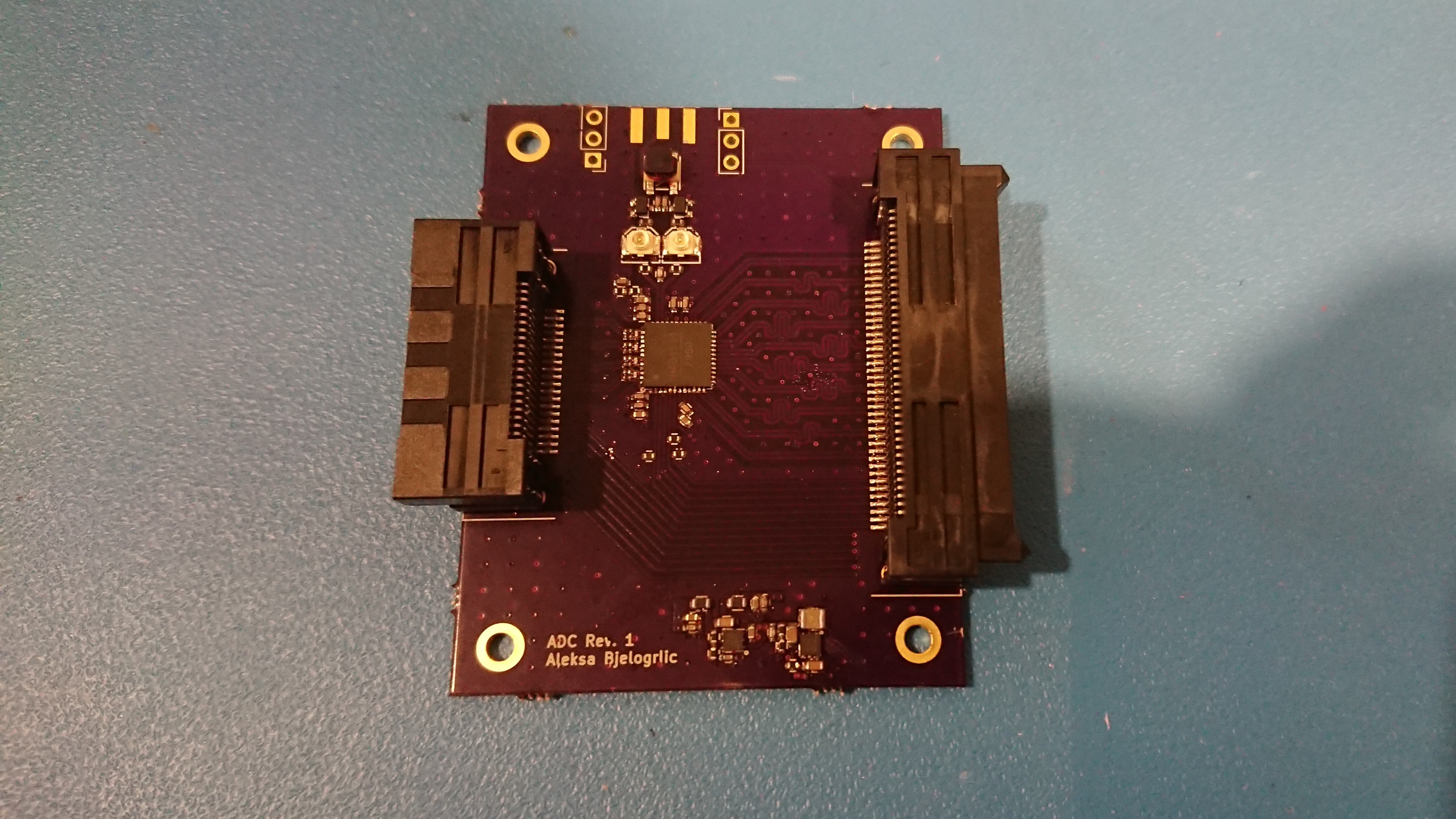
Loads of pretty squiggles on this one! They're pretty functional too, as they strategically add extra length on some lines so that every signal gets to its destination at the same time, preventing potential timing issues. Aside from that, that big connector on the right connects to the last board in the chain (this project's grand finale?... not even close!), the digital interface. This board can't be tested until the digital interface is built, so fingers crossed it all works!
Thanks for giving this post a read, and feel free to write a comment if anything was unclear or explained poorly, so I can edit and improve the post to make things clearer!
Discussions
Become a Hackaday.io Member
Create an account to leave a comment. Already have an account? Log In.