 Aleksa
It was time to see if the third time really was the charm and test the newest revision of the front end! The first task was to test the front of the front end (FFE) - the coupling circuit, attenuators and input buffer.
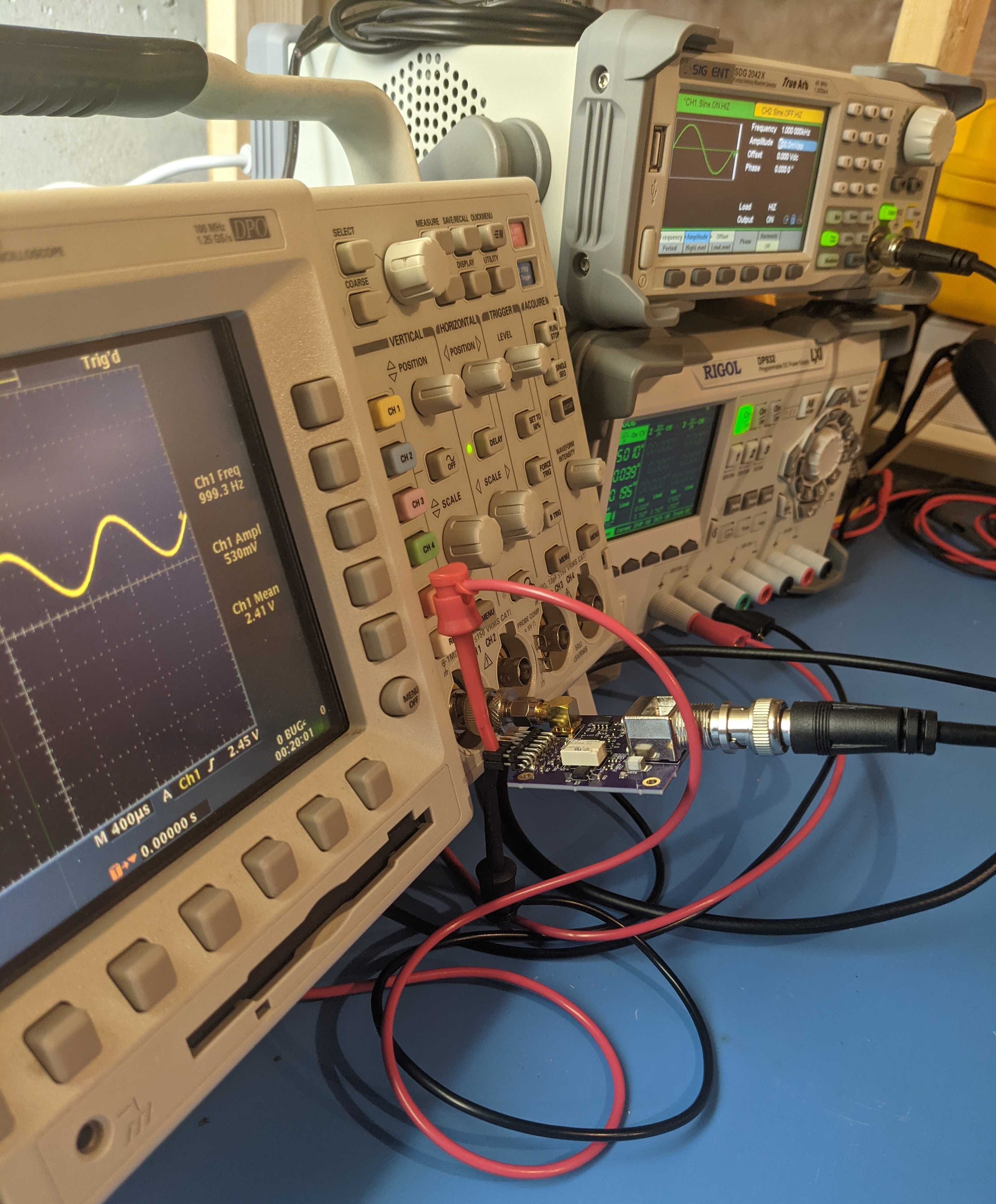
Look ma no probes! I started off by verifying the DC bias voltage at the output, which was just about the 2.5V I expected. The exact value of the bias voltage isn't important as it will be matched by the trimmer DAC once the channel is calibrated. I tested the AC coupling by adding a DC component to the signal, which caused no change to the DC voltage at the output. Next, I enabled DC coupling and confirmed that this DC component was now added to the bias voltage at the output. I then measured the DC gain, which was just under unity. After the coupling tests, I switched on the attenuator and was greeted with a flat output - no oscillations this time! I cranked my function generator to the highest voltage it could do, and lo and behold I could see the signal again, now attenuated by a factor of 100.
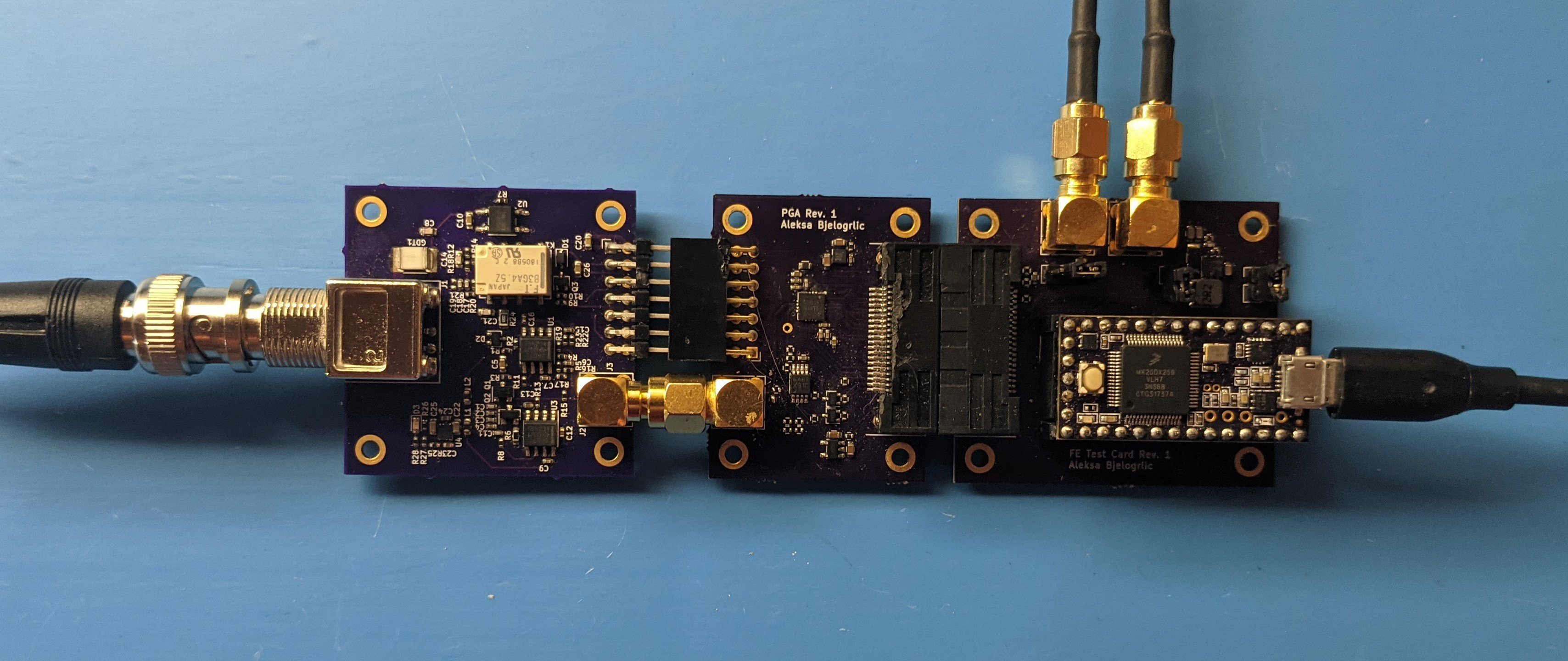
I then connected the FFE to the PGA and used the front end tester board to test the frequency response of the whole front end. I did this to avoid loading down the FFE’s buffer circuit with the high input capacitance (13 pF) of an oscilloscope input.
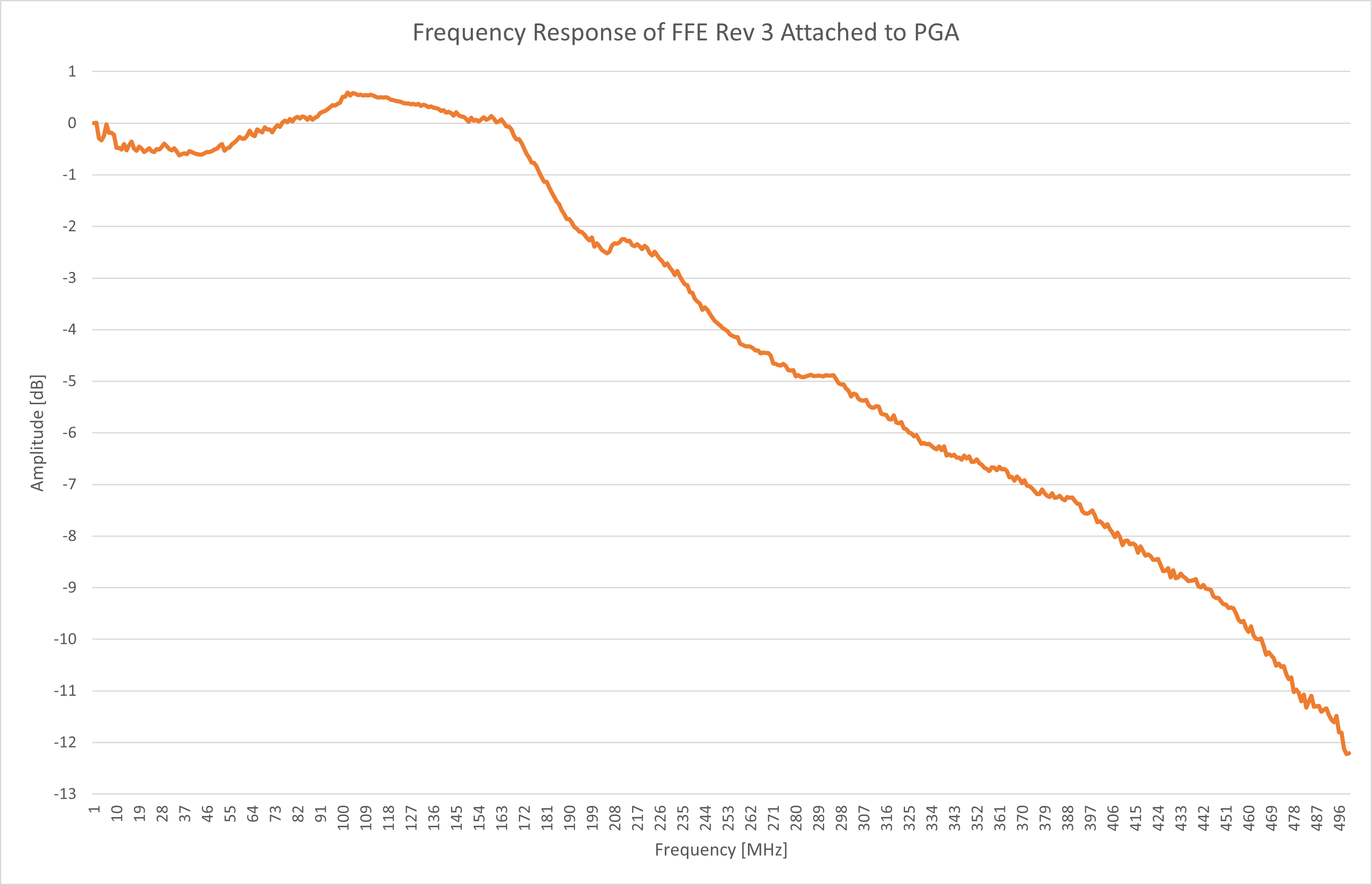
The frequency response certainly looked more promising than the previous attempts! The bandwidth was about 230 MHz, out of the 350 MHz promised by the simulations. This alone wouldn’t be too much of an issue if I scaled back the bandwidth requirement to 200 MHz. The real issue here is the flatness of the response, which is over +/- 0.5 dB when it should ideally be +/- 0.1dB. That means that on a scope with this front end, a 100 MHz clock would look 10% larger than a 32 MHz clock!
These peaks and valleys in the frequency response could have been caused by parasitics (unwanted inductance and capacitance) in the layouts of the two boards and in the connection between them. To reduce these parasitics and improve the bandwidth and flatness of the frequency response, I combined both FFE and PGA into one front end board, moving all the parts closer together to shrink the layout.
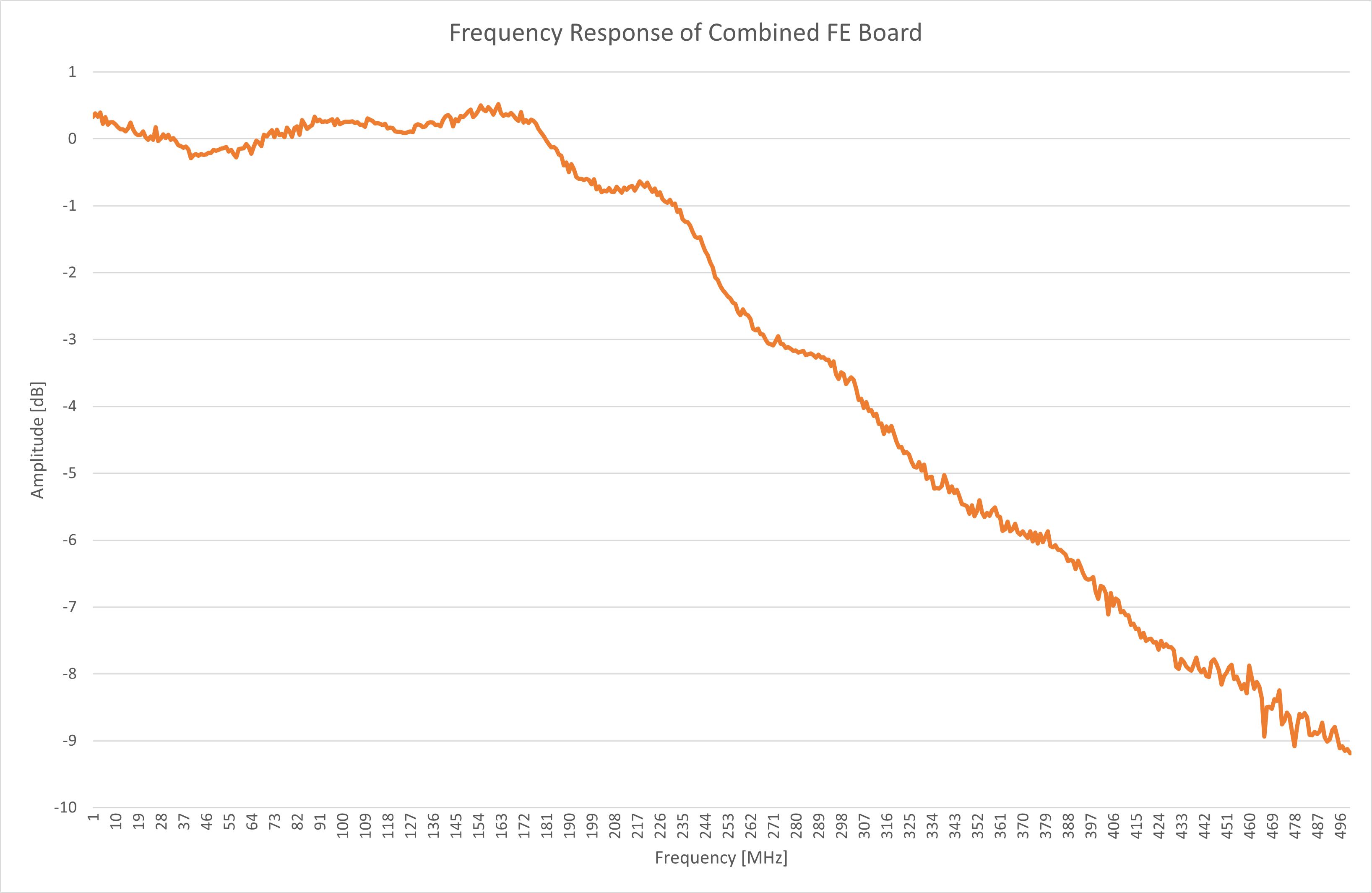
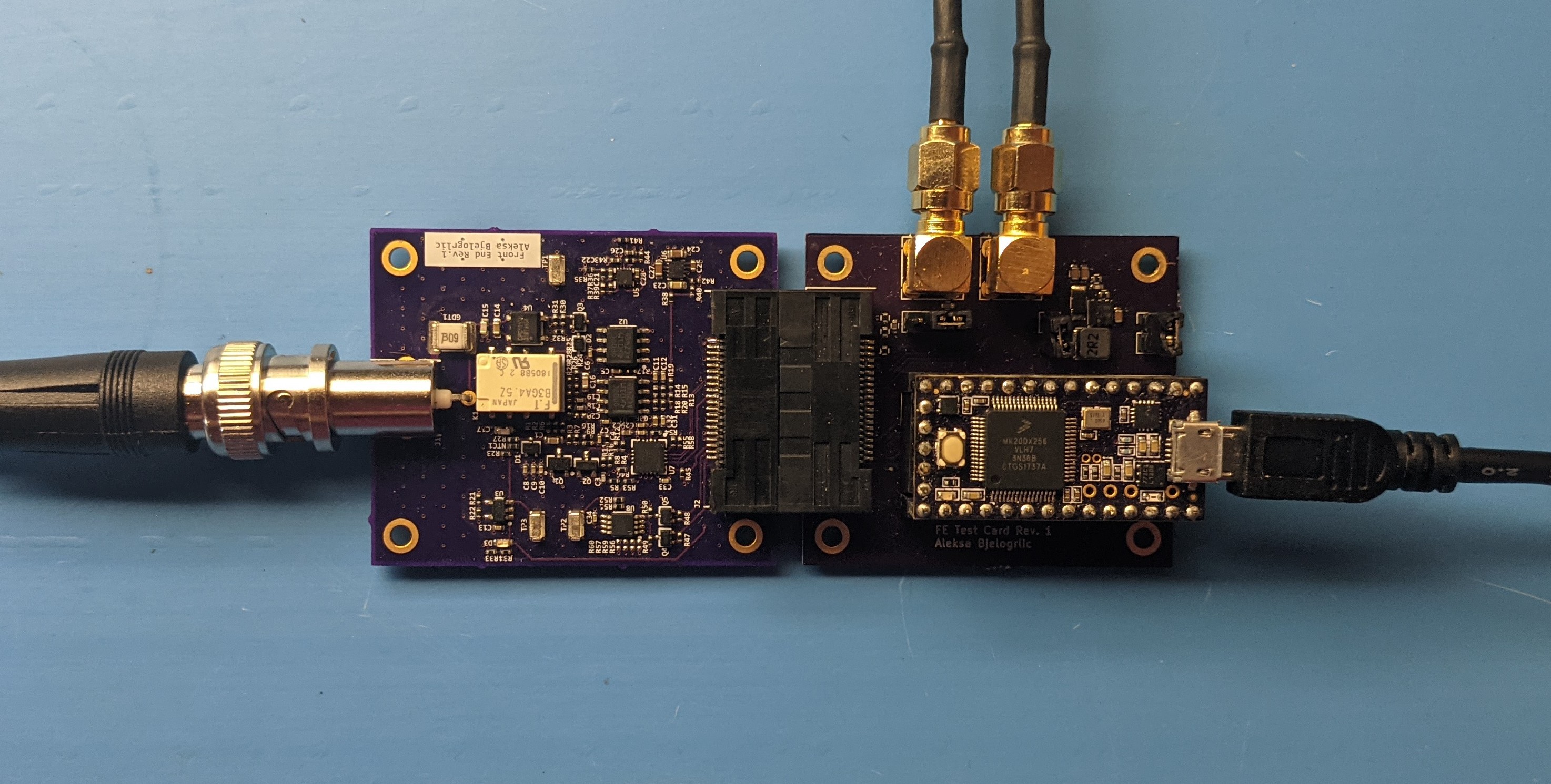
This new board improved the bandwidth to 260 MHz and the flatness to 0.25 dB. This was clearly a step in the right direction, but also showed that the likely culprits were the components on the board. I resolved to tweak the component values to improve the response later, but was satisfied enough to keep this design and continue on to a very exciting new development in this project - breaking the 1 GB/s barrier!
Thanks for giving this post a read, and feel free to write a comment if anything was unclear or explained poorly, so I can edit and improve the post to make things clearer!
Discussions
Become a Hackaday.io Member
Create an account to leave a comment. Already have an account? Log In.