 Aleksa
We've gone through a lot of hardware over these last 14 project logs! Before we leave the hardware hobbit hole to venture to software mount doom, let's take a look at the map of middle earth that is the block diagram of the whole system.
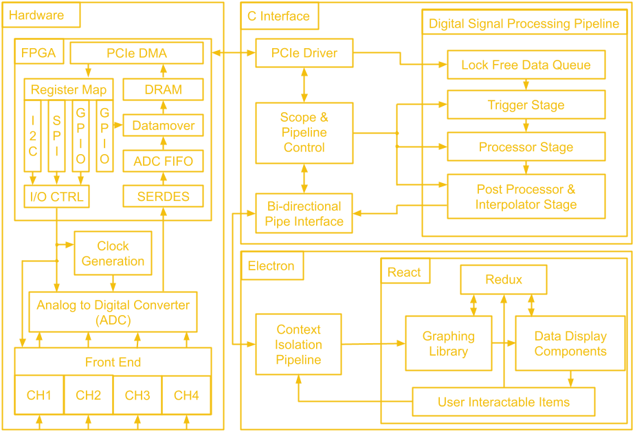
The first block we will tackle is the FPGA. The general structure is quite similar to the last design, there is ADC data coming in which gets de-serialized by the SERDES and placed into a FIFO, as well as scope control commands which are sent from the user's PC to be converted to SPI and I2C traffic. Since we don't have external USB ICs doing the work of connecting to the user's PC, this next part of the FPGA design is a little different.
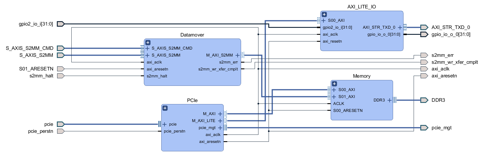
There is still a low speed and a high speed path, but instead of coming from two separate ICs, both are handled by the PCIe IP. The low speed path uses the AXI Lite interface, which goes to the AXI_LITE_IO block to either fill a FIFO which supplies the serial interface block or to control GPIO which read from the other FPGA blocks or write values to the rest of the board. On the high speed path, the datamover takes sample data out of the ADC FIFO and writes it to the DDR3 memory through an AXI4 interface and the PCIe IP uses another AXI4 interface to read the sample data from the DDR3 memory. The reads and writes to the DDR3 memory from the AXI4 interfaces are manged by the memory interface generator. The memory here serves as a circular buffer, with the datamover always writing to it, and the PCIe IP always reading from it. Collision prevention is done in software on the PC, using GPIO data from the low speed path to determine if it is safe to initiate a read.
With the deadline of the Hackaday prize fast approaching, I have called my friend Andrew out of retirement to write the rest of the software project logs. He worked on the software far more than I did, so he can give you a better overview of it! Plus he's not a chronically slow writer like I am, two project logs a month isn't too bad right?!
Next, we will question our life decisions as we begin ascending up the slope to Sauron’s domain and talk about the C interface implementation. The data is moved over PCIe by the PCIe IP's driver, also provided by Xilinx. PCIe is notoriously quite difficult to properly implement on the software side (quite the opposite from its hardware requirements) and while we considered writing a custom driver, we found that the off the shelf driver fit our requirements splendidly. This allowed our efforts to be focused elsewhere.
The driver itself passes the data to two separate sections of our C program. The first is the scope control mechanism. This is part of our bi-directional control system that allows the scope to tell the GUI the current state of the hardware (more on that in a later post), while allowing the user to change said state. Certain settings, such as voltage ranges, are not only software display options, but actually result in hardware changes in order to enable more granular reading of data.
The other data that the driver handles is, of course, the readings of the scope itself. This data takes a slightly different path as it requires some processing that would traditionally be done on the on board processor on a scope. The data first enters a queue, a circular buffer that gets processed each time it receives enough data. Specifically, this circular buffer is being analyzed for a possible trigger event, such as a falling/rising edge, as called in traditional scopes. This is such that the software knows when to lock in the data for presentation to the user.
Once a trigger event is discovered however, it then passes to the post processing and the interpolation stage. We process the data internally to make sure it conforms to the voltage and time scales expected according to the scope’s current state, and interpolate missing data based on sinx/x interpolation, the standard in oscilloscope design. You might notice that about half of the processing block is not directly related to hardware itself, but is actually present solely to ensure that the data can be accurately displayed to the user in the GUI. This is one of the challenges of such an implementation, where different components that are not self contained within the scope hardware have to sync up and communicate seamlessly.
Once the data has been processed, it is passed to the bi-directional pipe interface, where we once again meet up with our scope state information, ready to be passed onto our GUI (once again, more on that in a future post). In order to understand the choices we’ve made however, it is important that we explain exactly what our data pipeline is. On Linux we use UNIX Sockets, a quite simple, packet based IPC protocol that will be familiar to anyone that has had to make two programs talk before. We initially used a single bi-directional pipe. This brought about some challenges but with some timing sync logic, it worked out.
Then we looked at implementing the Windows logic. On Windows, the equivalent is something called Named Pipes. These do not really support bi-directional data transfers. The more suggested path, however, is just two parallel one way pipes. Upon testing we didn’t see any performance degradation on the Electron side. Turns out web browsers are quite good at handling packets, who knew? We also changed the Linux implementation to be the same, just to be able to reuse as much code as possible. The other interesting fact we discovered is that, in trying to keep the packets lean, we ended up with quite poor performance on the GUI side. It turns out that on Windows, there’s a upper limit on the top speed of packet delivery, a sort of “next bus” problem.
This does not change regardless of how much data you pack into one packet, up to a maximum limit. As such, the pipe towards the GUI packs enough data such that if we fill every available “bus”, we achieve 60fps on the display. The GUI app reads the header of the packet to figure out the beginning and end of actual data versus state updates and separates it as such for processing. On the receiving side, things are very similar. In order to ensure the system stays synced, the GUI also sends overloaded packets to the C program, to keep the side consistent, even though scope commands don’t technically call for this level of data density. Similar to the GUI side, the C program reads the header to know which commands were sent, compares them to a known look up table converting our internal identifier and value to a known “state”, and sends that state down the driver and to the FPGA to work its magic! And that’s all folks. Tune in next time for a deep dive into the Electron app and the GUI.
Thanks for giving this post a read, and feel free to write a comment if anything was unclear or explained poorly, so I can edit and improve the post to make things clearer!
Discussions
Become a Hackaday.io Member
Create an account to leave a comment. Already have an account? Log In.