 Arnov Sharma
Project's video-
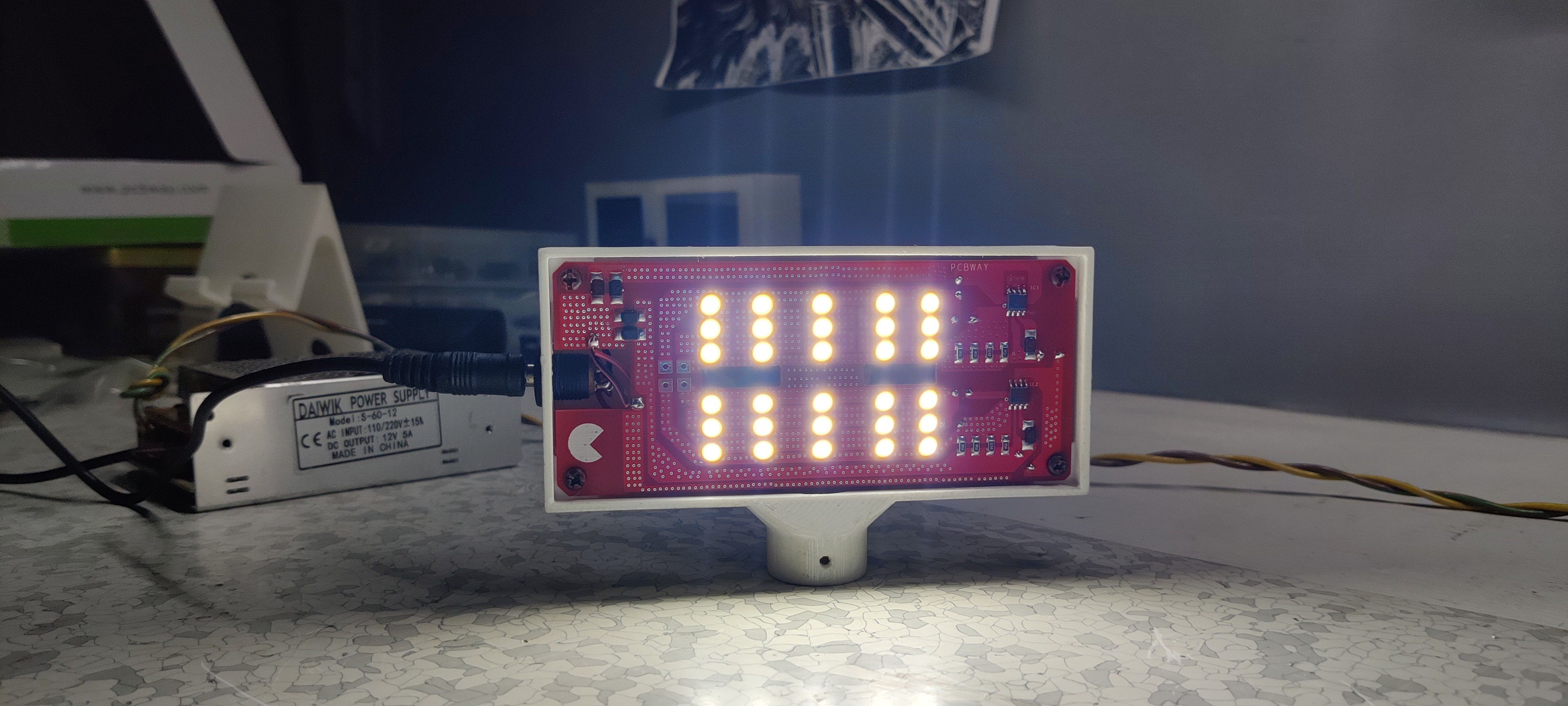
Commercially available light costs above 50$ (good ones) but why spend money on them when you can make your own Studio Light, Body can be made from a 3D Printer and the circuit can be manufactured by a PCB manufacturer.
But an Important question "Do these LEDs produce a lot of heat?"
Yes, these LEDs produce a lot of heat so why I'm not using MCPCB (metalcore) instead of FR4 (fiberglass) for making a better-LED PCB that can disperse heat better than FR4 Board.
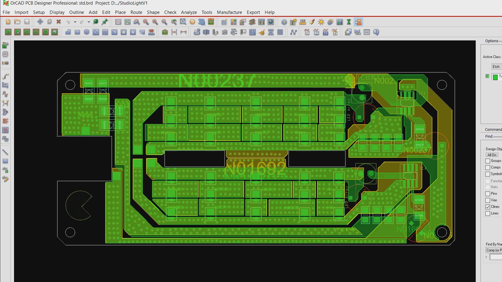
You see, I have added lots and lots of Via in this PCB, these Via will conduct heat from the top side and transfer that heat to the bottom portion which will result in Heat getting Disperse equally. Then at the backside, there's a 12V Mini DC FAN which cools down the PCB heat.
Apparently, Metal PCBs or MCPCBs are not $$$ wallet-friendly and if I have used a metal PCB in this project, I also have to use another FR4 board for LED Driver IC setup. So I saved a lot by making a single PCB that contains the LEDs and Driver IC setup.
Also, the Body of this light is made from PET-G which is quite a durable plastic so overall, this DIY Studio Light can sustain heat.
So in this post, I'm gonna show you guys the whole building process of this DIY Studio Light, so tight your seat belts and enjoy the ride.
 Pure Engineering
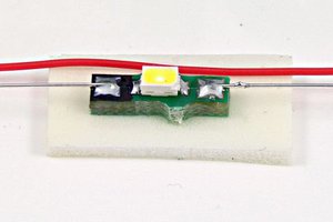
 Paul Stoffregen
 Sean Francis N.