Now that the basic switching circuits for the LEDs have been devised some maths is needed to determine resistor values and total current draws so the appropriate parts can be ordered. I could probably select these based on a random guess and it wouldn't hurt, but it's nice to know the effect of resistors selection on the project.
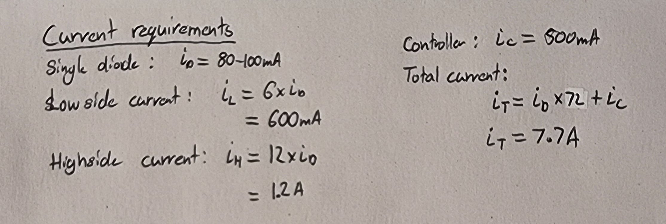
Current Requirements
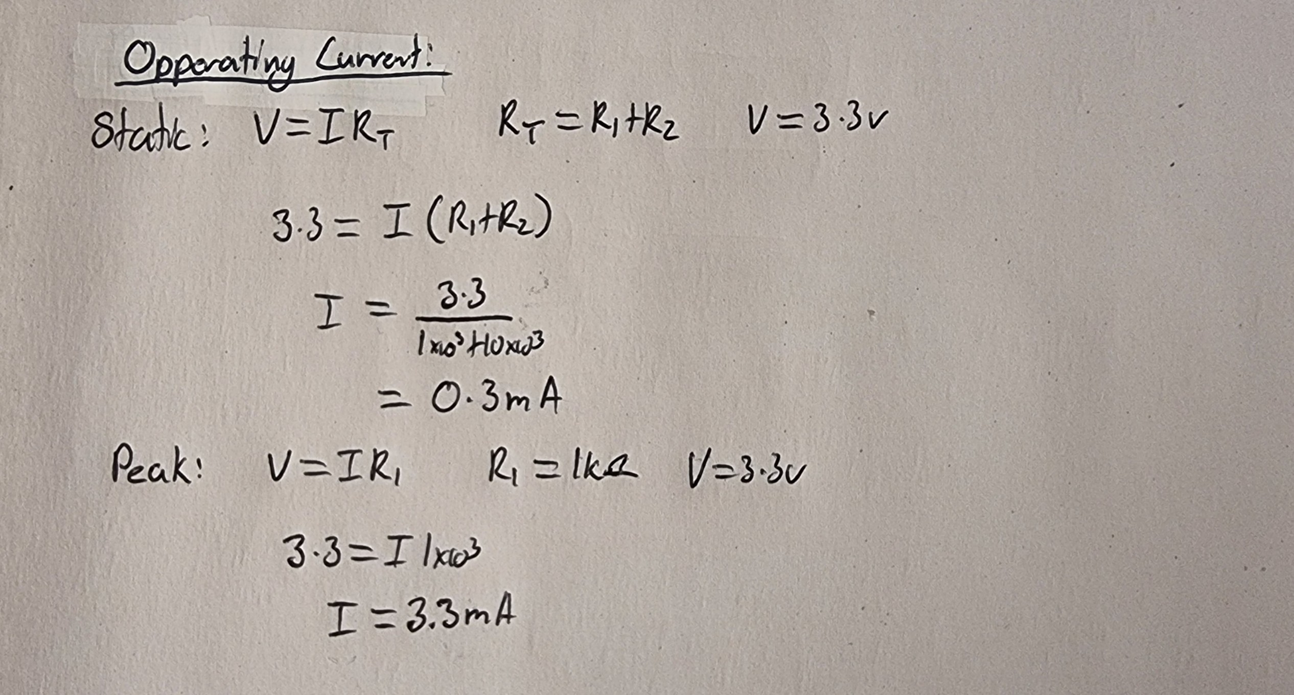
First off let's start with the current requirements for the driving circuits, a nice warm-up before we get into some more serious maths:
Based on this, an operating voltage of 5V, and a control voltage of 3.3V the following devices were selected for the control circuits:
- N-Channel MOSFET: FQU13N06LTU-WS (https://www.digikey.de/product-detail/en/FQU13N06LTU-WS/FQU13N06LTU-WS-ND)
- P-Channel MOSFET: FQU8P10TU (https://www.digikey.de/product-detail/en/FQU8P10TU/FQU8P10TUOS-ND)
- BJT: KSC1815YTA (https://www.digikey.de/product-detail/en/KSC1815YTA/KSC1815YTACT-ND)
I'm no expert so I don't know if these are the perfect parts for the job, but they should suit my purpose.
You may have noticed the 7.7A draw when everything is turned on at the same time, this is expensive and not very feasible. Instead, I picked out the most reasonably priced power supply that can turn on a significant number of LEDs at once. Which managed to be the SWI25-5-E-P5 (https://www.digikey.de/product-detail/en/SWI25-5-E-P5/102-4200-ND). With an output of 4A max at 5V, it should be able to turn on 1/3 to 1/2 of the LEDs at any one time, which is more than enough considering their brightness.
Low side driver
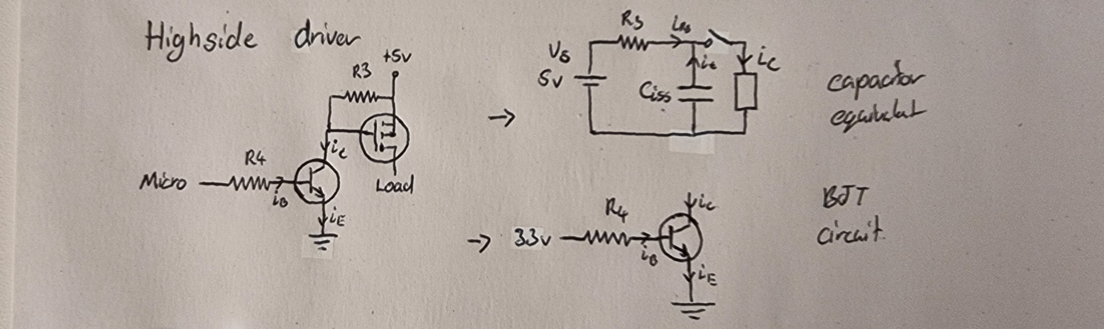
Now let's move on to the low side driver circuit. I recently read that one of the downsides of using MOSFETs for driving circuits is their relatively high input capacitance, which can impact high-frequency switching, and since I want to drive these LEDs with a PWM signal some investigation is in order. So to start, let's begin with some pretty pictures.
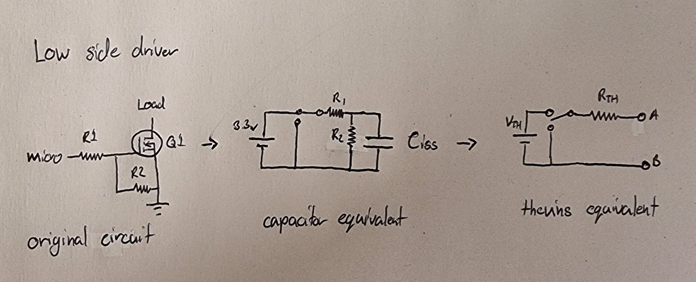
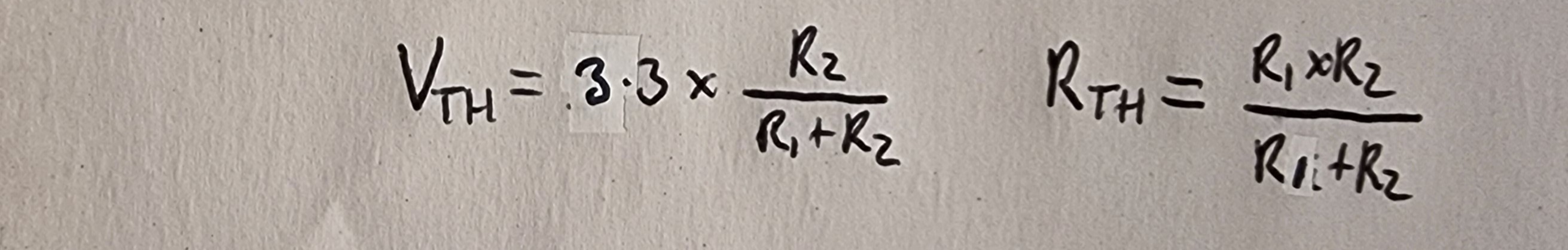
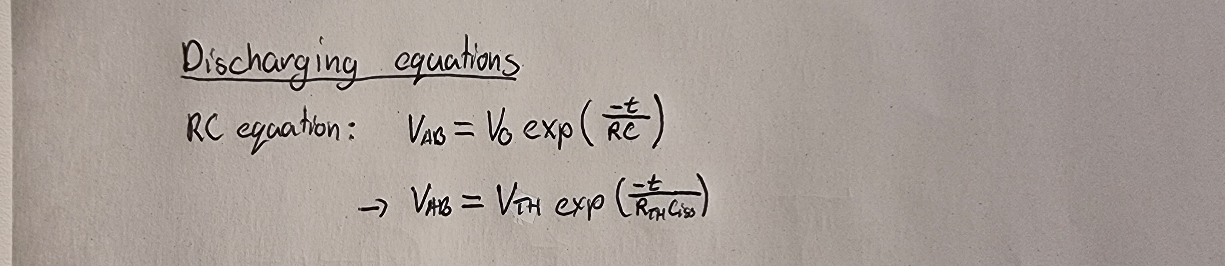
From the Micros point of view, the transistor is just a capacitive load. When this capacitive load reaches certain voltage levels it switches on or off based on the transistors gate threshold voltage. So for the circuits, we have replaced the transistor with a capacitor. The circuit can be simplified even more by replacing the source and resistors using Thevenin's equivalent circuit, reducing the calculations to a basic RC circuit, reducing the complexity of the maths. These equivalent values are as follows:
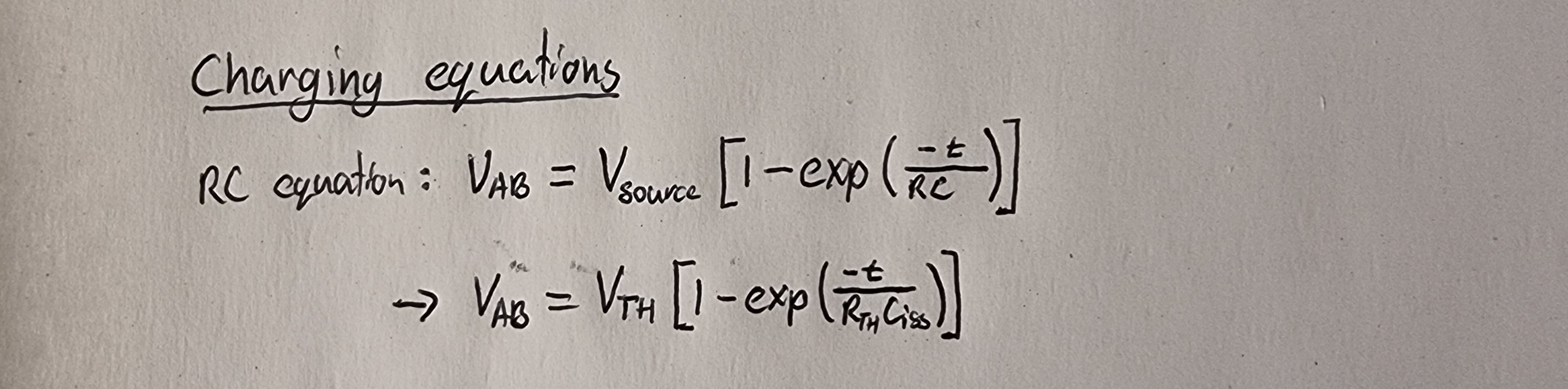
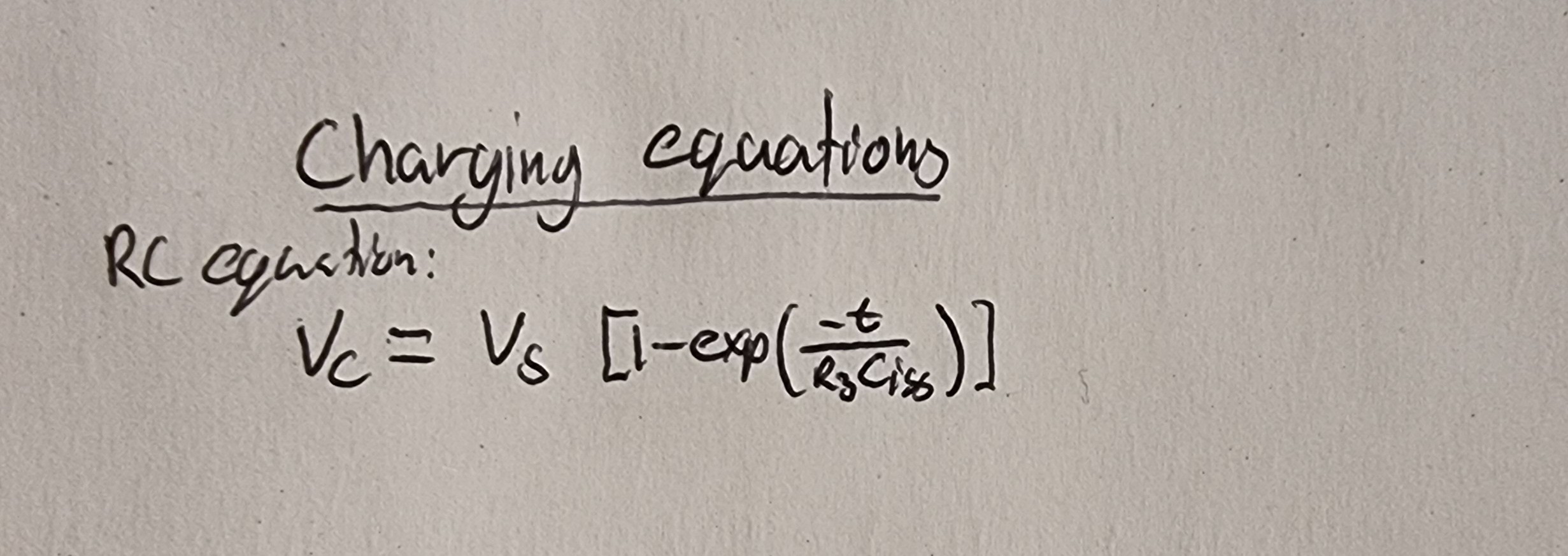
Using these in a basic RC charging equation gives:
And the same for the discharging equation:
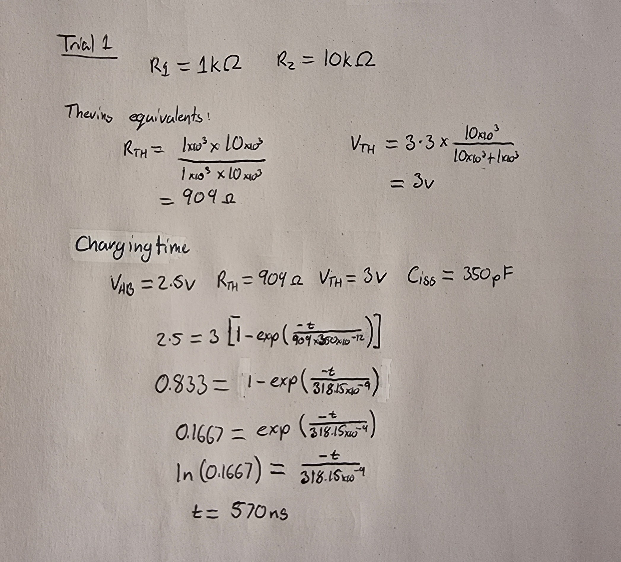
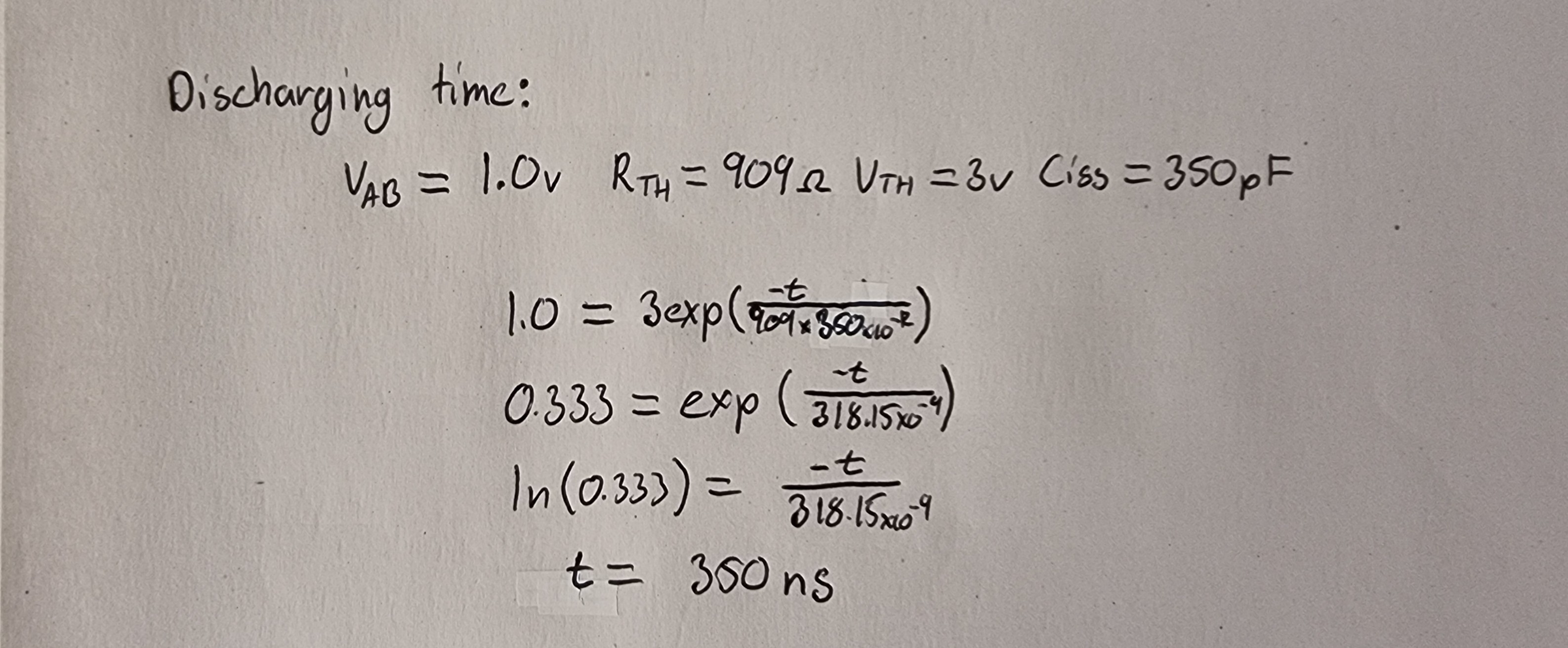
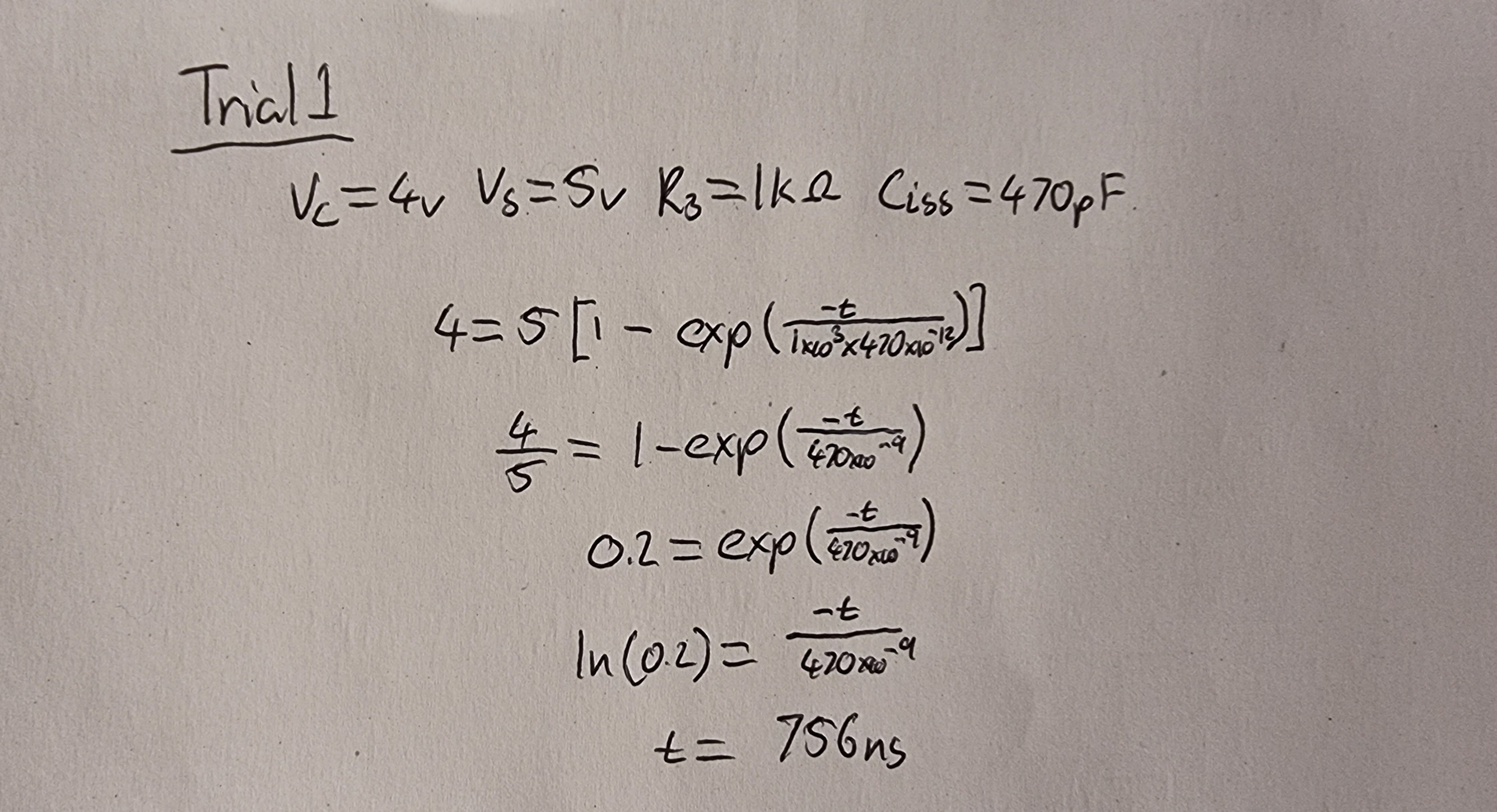
Using these two equations with two trial resistor values, the input capacitance of the MOSFET, switching voltages and solving for t can give us the total time required to switch the transistor on and off. Like so:
Combining these two times, and allowing for 5% of the total period to be used for switching gives the following maximum PWM frequency:
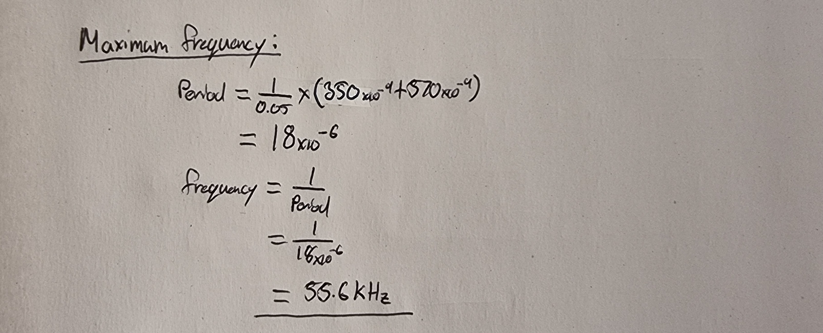
This frequency is well above the 10kHz maximum listed in the common PWM frequencies table for the ESP32 (https://www.espressif.com/sites/default/files/documentation/esp32_technical_reference_manual_en.pdf page 382), so in this regard the resistors are fine.
But, it's not just enough to know the switching frequency, we also need to check that the current draw doesn't exceed the supply capacity of the IO pins. This calculation is done below:
This current is within the limits of the ESP32 (https://www.espressif.com/sites/default/files/documentation/esp32_datasheet_en.pdf).
So it looks like resistor values of R1 = 1k Ohm and R2 = 10k Ohm are suitable for this application. Finer tuning could be done to optimise the switching time or current limiting, but since this is my first attempt it gives me some leeway on either side.
High side driver
While the circuits for the high side driver has a few extra parts, it's actually a little easier since it can be broken into two simple circuits:
The BJT is only used for discharging, so we will leave that for the end and start with the MOSFET charging equation like in the previous calculations:
This is simpler since we no longer need to use Thevenin's equivalence to solve it. So we will trial a resistor value straight away and see the results:
This switching time is a lot higher than for the P-channel MOSFET and that can be attributed to its larger input capacitance. The time could be reduced using a lower resistor value, but this would create a larger current draw when in operation so we will leave it as it is.
Since BJT's operate on current flow instead of voltage levels the discharge equation is even more simple. We can calculate a current based on the desired switching time, which in this case will be 100ns creating a total switching time a little less than that of the low side driver. This is done using the fundamental capacitor equation like so:
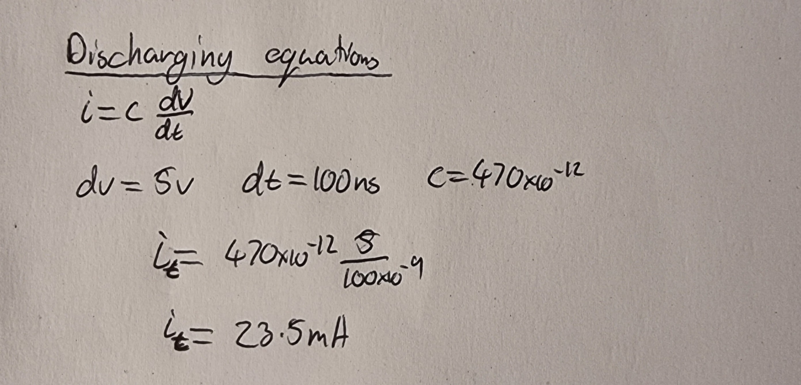
This current along with the Beta value of the BJT, base-emitter saturation voltage and the current flowing through resistor R3 can be used to calculate the base current required to switch on the circuit. Which is done as follows:
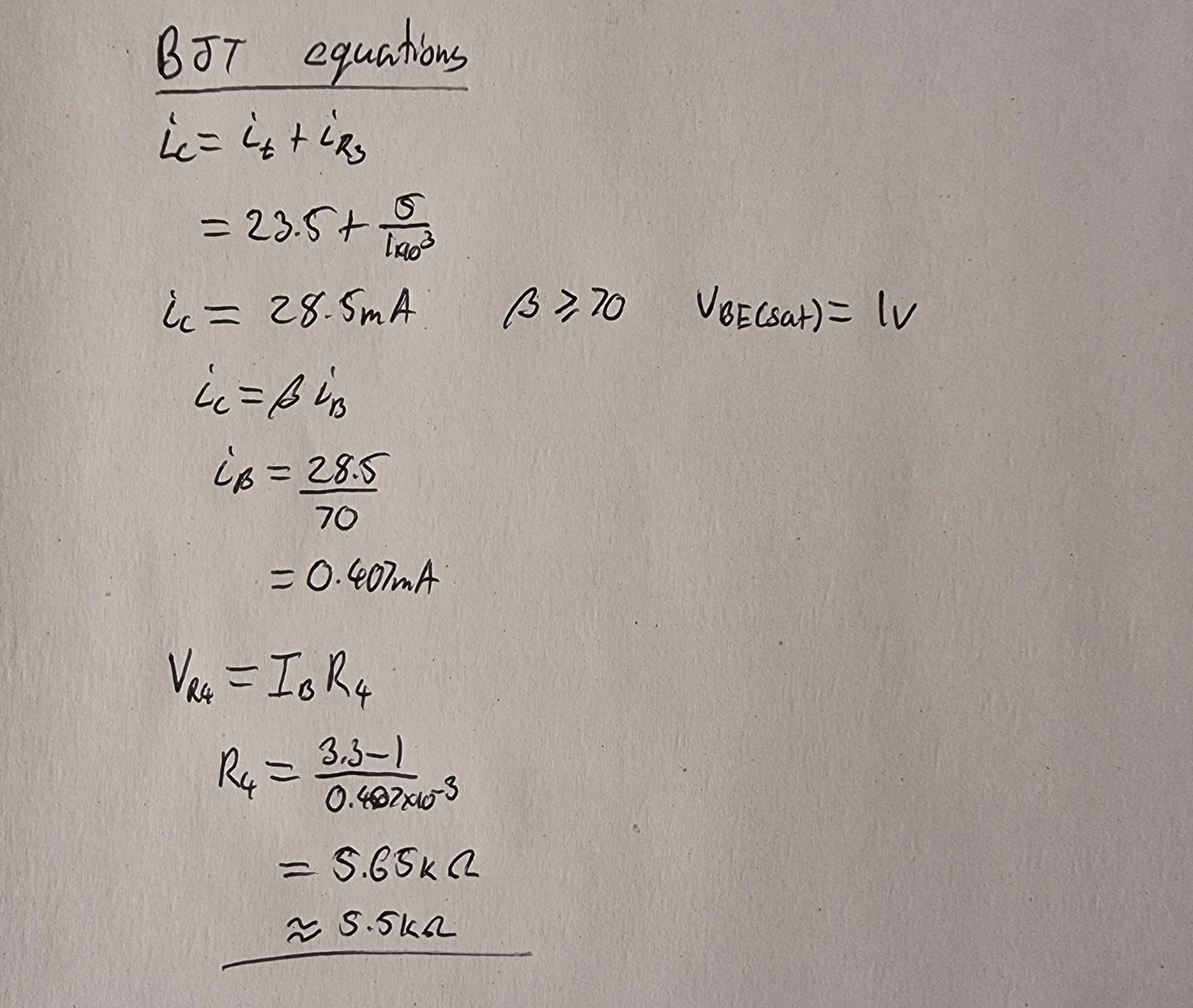
As seen above the base current can then be used to calculate the resistor value R4. Since both the switching frequency and the IO pin current are below those in the low side driver no further calculations are required.
From this, all the parts have been determined so a final list can be compiled and all the parts ordered, but I'll leave that for the next log :).
Discussions
Become a Hackaday.io Member
Create an account to leave a comment. Already have an account? Log In.