 davedarko
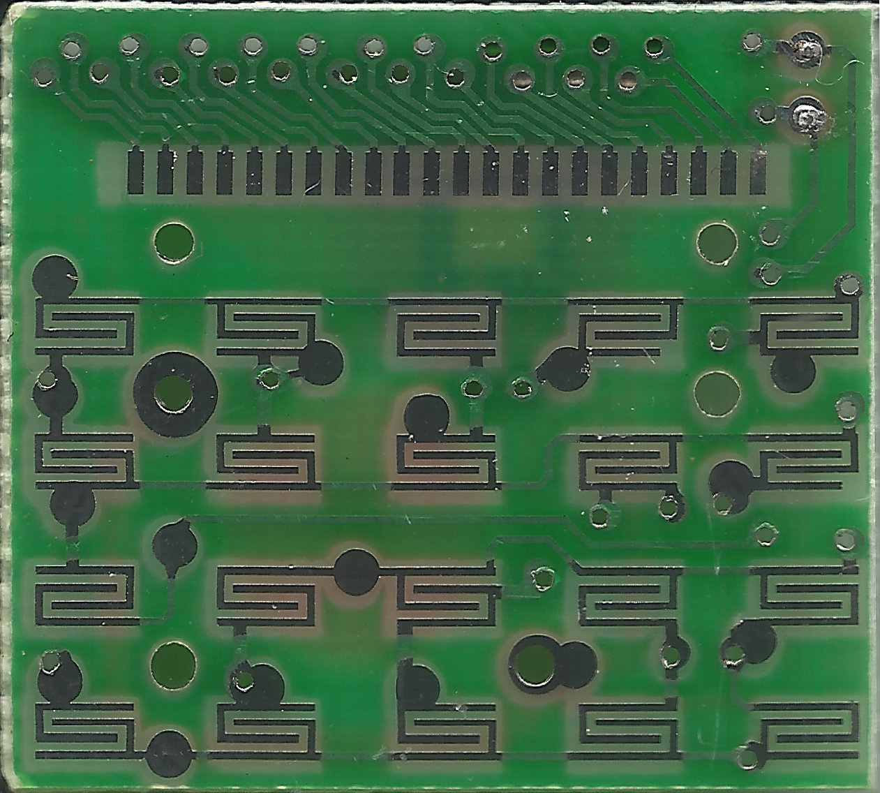
To make a replacement PCB you first have to know everything you can about the old PCB. Looking for my scanner I found a different one and used that instead. It was surprisingly easy to just plug it into my computer and scan without installing any ubuntu drivers, nice. After some tweaks in GIMP I was looking at this, the important side of the PCB with SMD pads that connect the LCD and the button matrix.
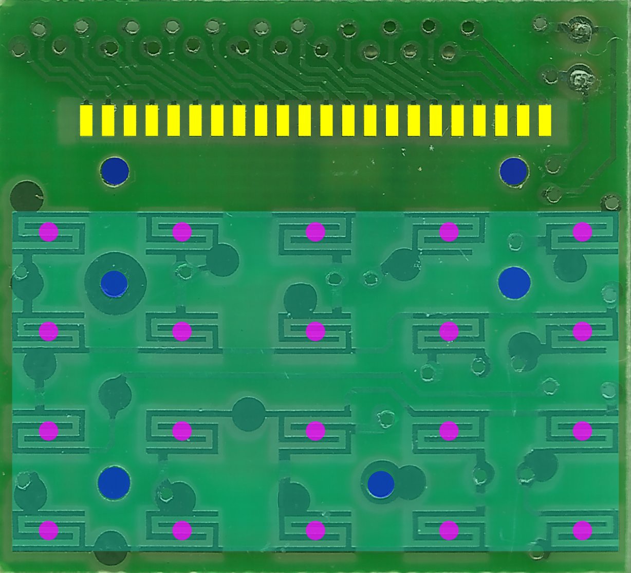
The next step for me then was to import the PNG into inkscape, mainly to draw the new shape of the PCB and get all drillholes and button positions, as well as the LCD pads. The pads are spaced 0.9mm from each other. I learned that by measuring 18.9mm from first pin to last pin and dividing that by 21. Nice.
There are 1.1mm, 1.2mm and something around 1.4mm drill size holes on the PCB, either for screws or mounting poles of the plastic case. After pushing things around and trying to find a center I ended up with this colorful layered image.
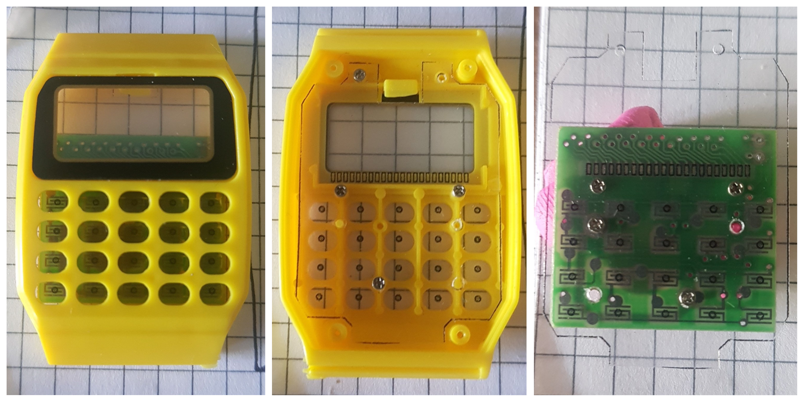
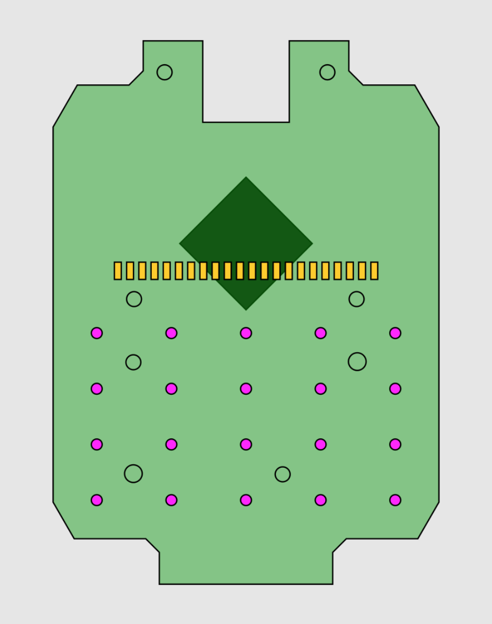
I continued with importing a photo of the case internals, so I can draw a new PCB shape with more real estate, using what I can get. We definitely want to add a side glowing LED and there are some free screw-holes that we can use. To test the PCB dimensions and mounting hole positions, I printed only the contours of all the elements onto a clear overhead projector foil. It helps to have small drill bits around, to probe the hole sizes.
Looks like the fit checks out :) Now I need to find out how to get that SVG into something that I can convert and work with in KiCad. Did you notice how many open source projects I've listed?
This is what the PCB now would kinda look like. I might remove the LCD holding tap and close that top opening as it does not really seem to do anything.
Discussions
Become a Hackaday.io Member
Create an account to leave a comment. Already have an account? Log In.