 Ken Yap
Now we complete the instruction processing by dealing with the upper 8 instructions, the ones that have the high bit on, comprising STO, STOC, IEN, OEN, JMP, RTN, SKPZ, and NOPF. In this version we don't implement JMP, RTN and SKPZ. Here is the Logisim design for the rest.
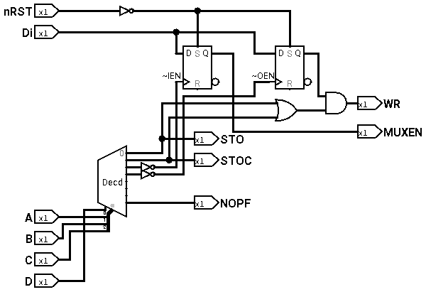
We use a 3 to 8 decoder/demultiplexer to enable one of 8 outputs when that particular instruction is selected. The D line is used to enable decoding for this group of 8. Unlike the TTL design I'm following, I intend to use an active high out decoder, the 74LS259, instead of the original active low out 74LS138. So the Write line is enabled using an OR gate whenever STO or STOC is executed. STO or STOC are also used in the Logic Unit to invert Do.
IEN and OEN are inverted and used to clock in the input data. The inversion means that the Di is clocked in at the falling edge of the IEN or OEN lines depending, meaning at the beginning of the next instruction. I was uncomfortable with using IEN and OEN to clock the D flip-flops this way but this is in fact how it's represented in the block diagram of the innards of the MC14500B. Note that the flip-flops are reset to IEN and OEN high with nRST.
Commentary on more use of Logisim: It's fairly easy to verify combinatorial circuit behaviour, but sequential circuits take more effort, because of the extra dimension of time obviously. It would be nice to have models for various TTL chips, but only a handful are supplied in the standard package. So the generic parts such as decoder, D flip-flop, etc. may differ from the actual part you hope to use. For example, in the diagram above the R and S lines of the flip-flops are active high but in the actual design, they will be active low. Hence the inverter for the nRST line.
Discussions
Become a Hackaday.io Member
Create an account to leave a comment. Already have an account? Log In.