 Lauri Pirttiaho
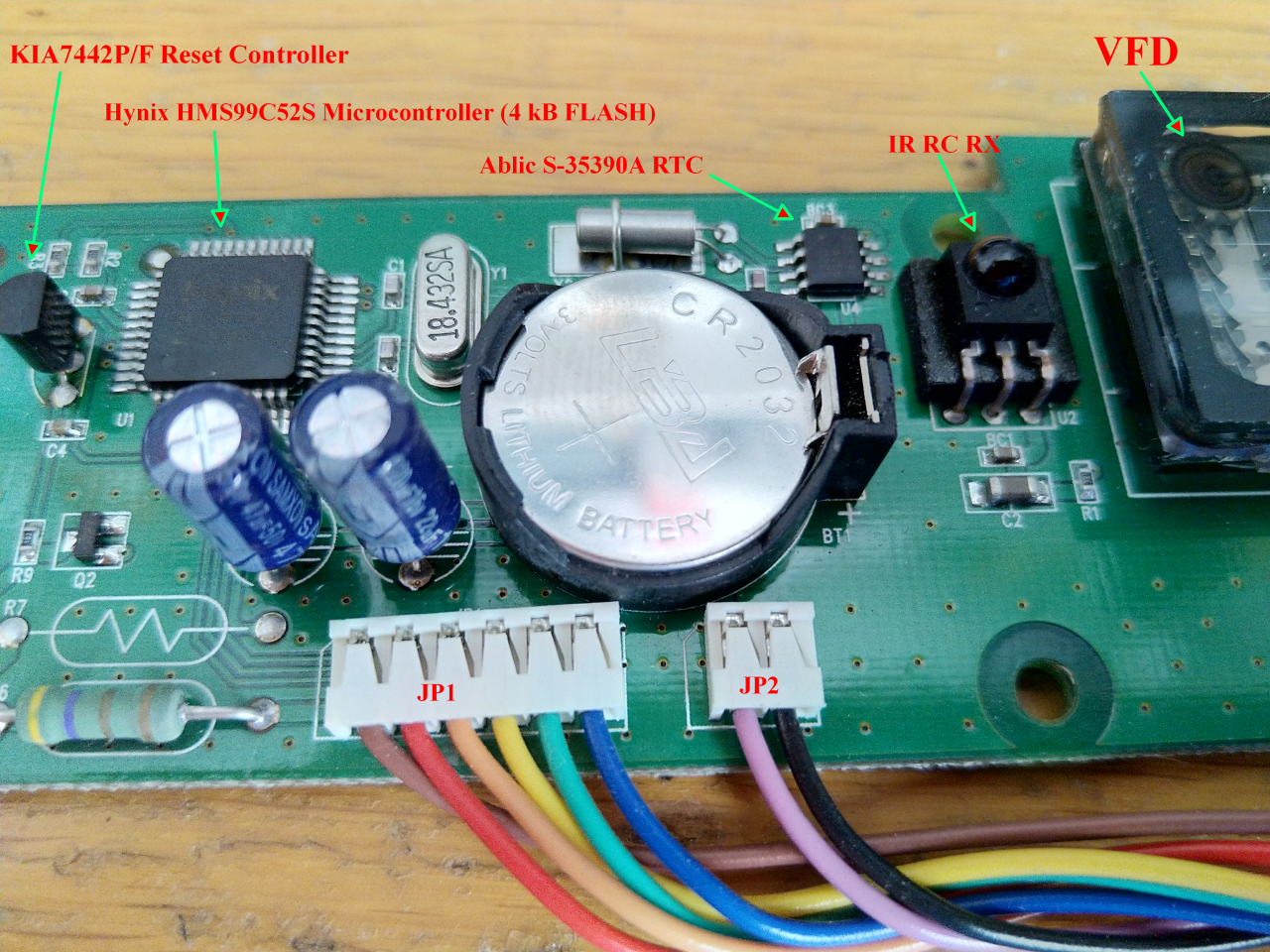
Connectors
- JP1
- Brown: Vcc (+5 V)
- Red: TXD (UART data from UI to main board)
- Orange: RXD (UART data from main board to UI)
- Yellow: GND
- Green: Connected to microcontroller T0/P3.4
- Blue: VFD HV (+17 V) - Connected to JP1-1(Purple)
- JP2
- Purple: VFD HV (+17V)
- Black: GND
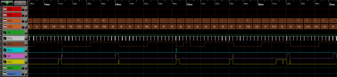
Protocol
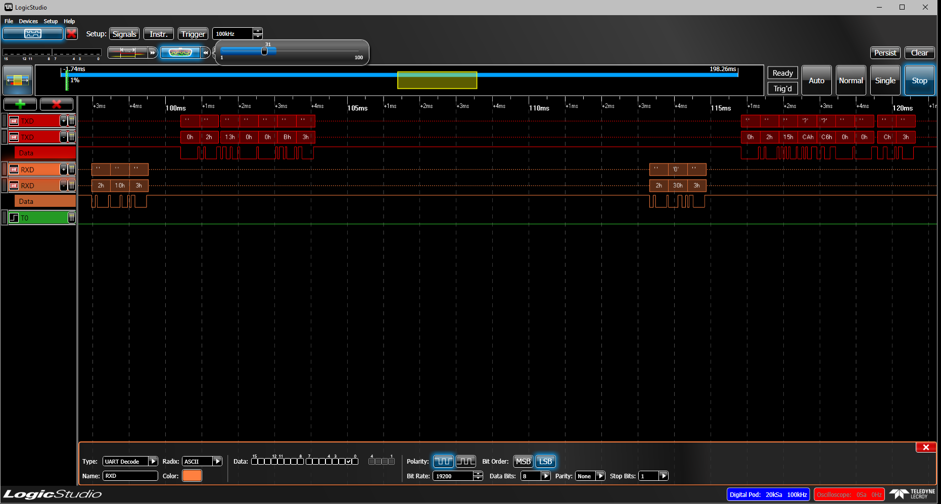
The UART settings are 19200 baud 8N1.
The communication appears to consist of <STX> <type|dlen> <data>{dlen} <ETX> packets where type is the high nybble of the second byte and dlen its low nybble giving the number of data bytes following it.
Display
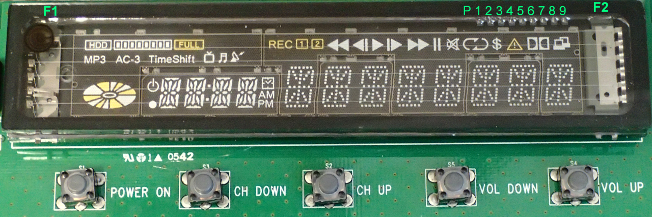
The filament voltage (F1 positive, F2 ground) is about 3.58 V, fed from +5V via 4.7 Ω resistor and a PNP switch, so that the current is about 225 mA. The filaments are tilted for DC drive.
The connector P[1:8] is:
- Serial data, clocked at rising edge of clock. Microcontroller pin P2.3. Possibly bit-banged SPI.
- +5 V
- Not connected. Appears to be serial data out from the CIG chip.
- Load strobe. Microcontroller pin P2.2. 400 ns pulse every 4 ms.
- <unknown> Microcontroller pin 2.1.
- Clock. Microcontroller pin P2.0. Rate 230 kHz, idle high.
- GND
- GND
- +16.6 V
The data appears to be 1:3 multiplexed, 128 bits (16x8) for each group.
The CIG chip is under the right hand side (raised) filament holder. Chip is bonded from two sides. Type unknown. This could be a 128-bit serial to parallel converter with high voltage outputs, similar to Supertex/Microchip HV583 (die bonding does not match the pads of HV583 so it likely is not that, though).
Writing to Display
Messages of type 9 are used to write to byte arrays that the on-board microcontroller uses to drive the VFD.
Message 0x02 0x9<len> <addr> <data_0>...<data_len-2> 0x03 writes the data bytes to array at the given address. Each of the three multiplexed data sets are 16 bytes long. Set 0 is at address 0x00, 1 at address 0x10, and 2 at address 0x20. Since one write is limited to 14 bytes of data the main board CPU writes each set with two writes: first 8 bytes to 0x[0-2]0 and then 8 bytes to address 0x[0-2]8. The first data byte of each set (0x[0-2]0) selects the grid and it is 0xC0, 0x3C, or 0x03 for sets 0, 1, and 2, respectively. The set 1 appears to contain largest number of segments and is probably for that reason allocated 4 outputs, while two other sets use 2 outputs. The rest (120) bits select the segments (1 on, 0 off),mapping of which will be determined soon.
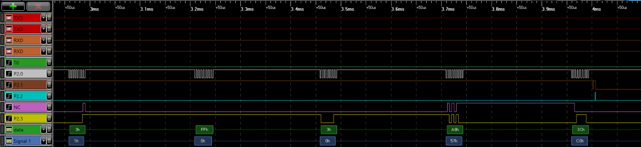
The on-board microcontroller uses SPI-like protocol (by bit-banging as there is no SPI HW in that microcontroller) and feeds the bits in reverse order to the CIG of the VFD as can be seen by comparing the bit patterns in the logic waveforms.
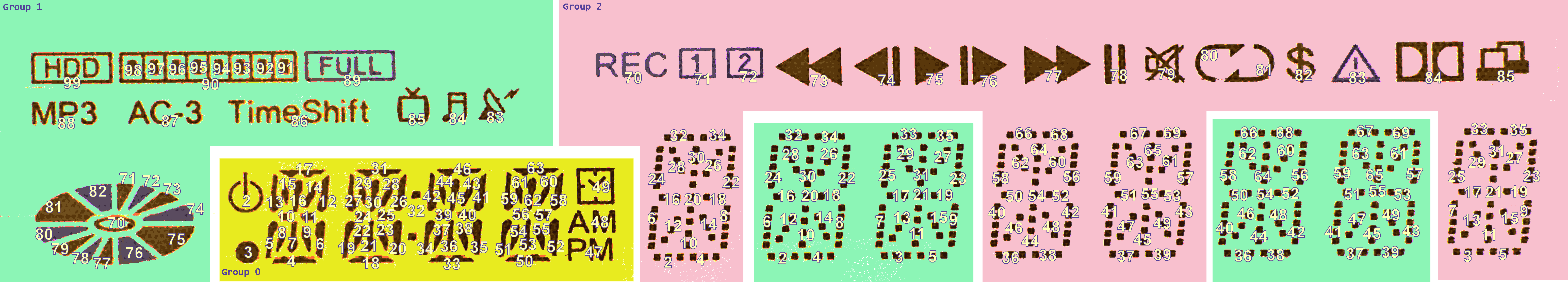
Mapping of the segments
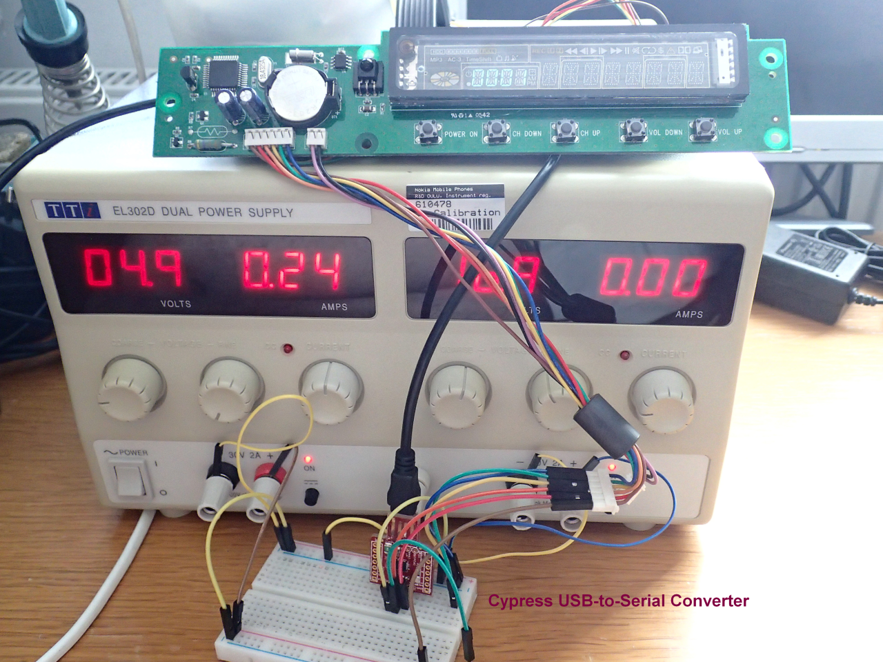
The display module was connected to a PC using a Cypress USB-to-serial break-out board, and a small Python script was used to step through all segments.
#!/usr/bin/env python3

from serial import Serial
from time import sleep
from sys import stdout

msgs = [
    [0x02, 0x99, 0x00, 0xc0, 0x00, 0x00, 0x00, 0x00, 0x00, 0x00, 0x00, 0x03],
    [0x02, 0x99, 0x08, 0x00, 0x00, 0x00, 0x00, 0x00, 0x00, 0x00, 0x00, 0x03],
    [0x02, 0x99, 0x10, 0x3c, 0x00, 0x00, 0x00, 0x00, 0x00, 0x00, 0x00, 0x03],
    [0x02, 0x99, 0x18, 0x00, 0x00, 0x00, 0x00, 0x00, 0x00, 0x00, 0x00, 0x03],
    [0x02, 0x99, 0x20, 0x03, 0x00, 0x00, 0x00, 0x00, 0x00, 0x00, 0x00, 0x03],
    [0x02, 0x99, 0x28, 0x00, 0x00, 0x00, 0x00, 0x00, 0x00, 0x00, 0x00, 0x03]
    ]

def set(line, segment, val):
    if segment < 56:
        msg_index = 2 * line
        byte = 4 + segment // 8
    else:
        msg_index = 2 * line + 1
        byte = 3 + (segment - 56) // 8
    bit = 7 - segment % 8
    if val:
        msgs[msg_index][byte] |= 1 << bit
    else:
        msgs[msg_index][byte] &= ~(1 << bit)
    msgs[msg_index][byte] &= 0xff
    return bytes(bytearray(msgs[msg_index]))

stdout.write('          ')
stdout.flush()

with Serial('COM7', 19200, timeout=1) as com7:
    for m in msgs:
        com7.write(m)
        sleep(0.2)
    sleep(1)

    for j in range(3):
        for i in range(120):
            stdout.write('\b\b\b\b\b\b\b\b\b\b')
            stdout.write('({:3d},{:3d})'.format(j,i))
            stdout.flush()
            com7.write(set(j,i,1))
            sleep(1)
            com7.write(set(j,i,0))
            sleep(0.3)
Following video shows the mapping:
and it is also described in the following diagram:
Discussions
Become a Hackaday.io Member
Create an account to leave a comment. Already have an account? Log In.