zpekic
The best way to test and illustrate new components is to put them into a "end to end" project. It is even better to be able to visualize what is happening, and for that purpose a video output component was reused from another project.
Here is the somewhat simplified schema of the top level file of the project, which is at the same time the test circuit:
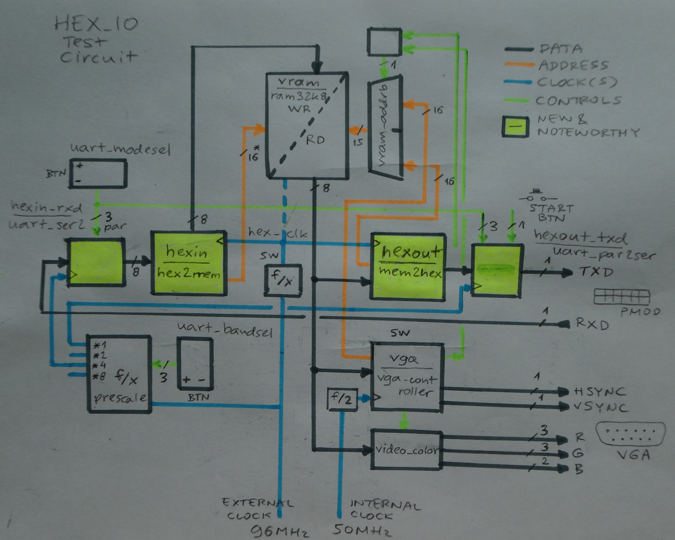
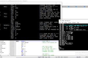
The "new and noteworthy" components are explained in the project logs. The dual port RAM is initialized with an image during build time (as is often the case with FPGA projects, for example, "firmware" for the system being implemented). During runtime, it can either be loaded with new HEX file stream, contents read as HEX stream, or both (not at the same time, switch(0) on Mercury board selects the mode).
Some other components visible on the schema:
- 50MHz internal clock - it is divided by two and fed as pixel clock to VGA, closely matching the need for 640*480, 50Hz refresh video mode
- 96MHz external clock - it is fed by "half can" on Mercury baseboard. All clocks in the project are derived from this one. Most importantly:
- Divided by multiples of 2, it becomes hex_clk that is fed to hexin and hexout components (max. 12MHz)
- Divided by constant, becomes the standard baudrate from 600 to 57600 Hz.
- vga_controller - it is able to display image in 2 different formats, selectable by switch(1). Given that both formats occupy less than the 640*480 resolution, a "hardware window" is displayed on static background, and can be moved in 4 directions using the buttons on the baseboard
- uart_modesel - simple 3 bit counter that allows selecting the UART mode (default at reset: 000 == 8 bit, no parity, 1 stop)
- uart_baudsel - simple 3 bit counter that allows selecting the UART speed (default at reset: 111 == 57600)
- vram_addrb - address MUX on the read side of the memory. Both vga_controller (to generated the image in the display window) and hexout (to assemble HEX character stream to output) need access to memory. Precedence is given to VGA, but if hexout manages to get access and flip the MUX to its side, it will keep it until the end of read cycle. This causes some "snow" on the image. It can be eliminated with a small speed tradeoff. Note that both components support full 16-bit address space, but the memory is 32k so A15 is dropped.
- vram - this is 32k*8 dual port RAM, intrinsic to Xilinx Spartan, but most other FPGAs will have it as standard component. It contains the image which can be changed via HEX file upload.
Top level entity description defines the use of hardware resources on the board. A/D, PS/2 and audio in/out are not used.
entity hex_io_mercury is
    Port (
                -- 50MHz on the Mercury board
                CLK: in std_logic;

                -- 96MHz external clock
                EXT_CLK: in std_logic;

                -- Master reset button on Mercury board
                USR_BTN: in std_logic;

                -- Switches on baseboard
                -- SW(0) -- OFF: accept HEX input, ON: generate HEX output
                -- SW(1) -- OFF: TIM-011 video (512*256, 4 colors), ON: V99X8 video (256*192, 16 colors)
                -- SW(2) -- HEX_CLK speed sel 0 (000 = trace mode, tracer is active)
                -- SW(3) -- HEX_CLK speed sel 1
                -- SW(4) -- HEX_CLK speed sel 2 (111 = 12MHz)
                -- SW(5) -- ON: Enable character echo trace for HEXOUT
                -- SW(6) -- ON: Enable write to memory trace for HEXOUT
                -- SW(7) -- ON: Enable error trace for HEXOUT

                SW: in std_logic_vector(7 downto 0);

                -- Push buttons on baseboard
                -- BTN0 - HEX input mode: move window right    ; HEX output mode: start output
                -- BTN1 - HEX input mode: move window left    ; HEX output mode: increment mode register
                -- BTN2 - HEX input mode: move window down    ; HEX output mode: select uart_mode
                -- BTN3 - HEX input mode: move window up        ; HEX output mode: select uart_baudrate
                BTN: in std_logic_vector(3 downto 0);

                -- Stereo audio output on baseboard
                --AUDIO_OUT_L, AUDIO_OUT_R: out std_logic;

                -- 7seg LED on baseboard
                A_TO_G: out std_logic_vector(6 downto 0);
                AN: out std_logic_vector(3 downto 0);
                DOT: out std_logic;
                -- 4...
Read more »
 spudfishScott
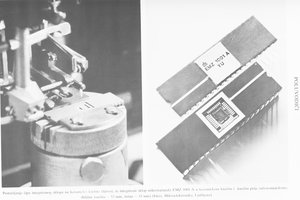
 Anders Dinsen